Mx410 data path block diagram, Mx410 data path block diagram -2, Figure 3-1. mx410 data path block diagram -2 – ADTRAN MX410 User Manual
Page 20: Mx410
MX410/MX412 System Manual
3-2
PRELIMINARY
61189500L1-1B
MX410 DATA PATH BLOCK DIAGRAM
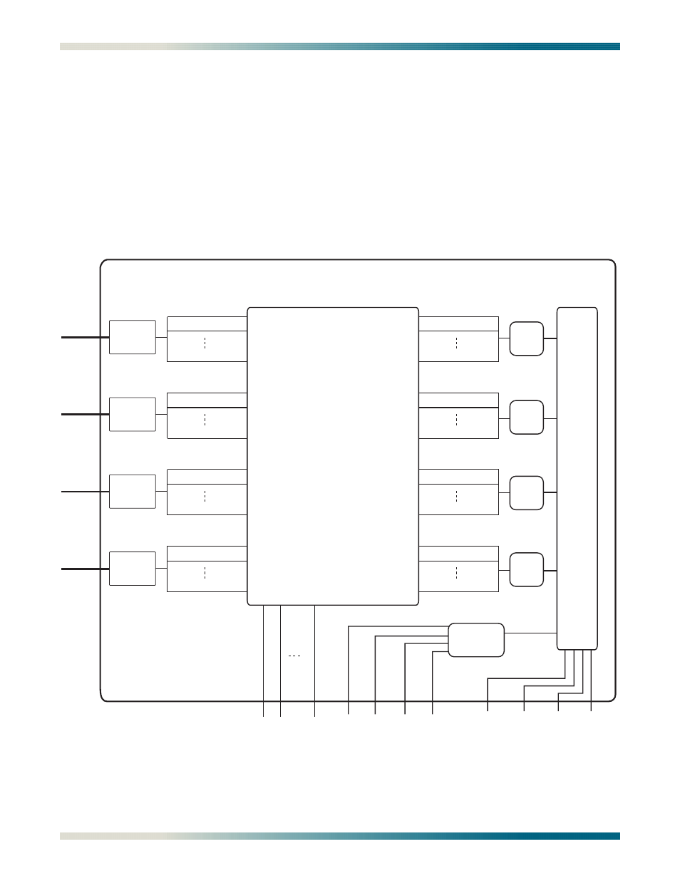
As shown in
, the MX410/MX412 contains a 1/0 cross connect that allows DS0s to
be mapped between four DS1s (12 DS1s on the MX412), four PPP ports, and a V.35 port. Refer
to
on page 5-32 for more information about using PPP.
Any DS0 in DS1 1 can be mapped to any DS0 in DS1 1-4, or any PPP port, or the V.35 port.
Any unmapped DS0 in a DS1 is filled with all ones. Therefore, if an entire T1 is unmapped,
framed all ones are sent.
The default mapping of the 1/0 cross connect is for all the DS1s to be unmapped and trans-
mitting framed all ones. No DS0s are dropped to the PPP or V.35 ports.
Figure 3-1. MX410 Data Path Block Diagram
V
.35 Port DS0 # 1
V
.35 Port DS0 # 2
V
.35 Port DS0 # 24
DS1 1 DS0 # 1
DS1 1 DS0 # 2
DS1 4 DS0 # 24
DS1 1 DS0 # 24
DS1 2 DS0 # 1
DS1 2 DS0 # 2
DS1 2 DS0 # 24
DS1 3 DS0 # 1
DS1 3 DS0 # 2
DS1 3 DS0 # 24
DS1 4 DS0 # 1
DS1 4 DS0 # 2
PPP 1 DS0 # 1
PPP 1 DS0 # 2
PPP 4 DS0 # 24
PPP 1 DS0 # 24
PPP 2 DS0 # 1
PPP 2 DS0 # 2
PPP 2 DS0 # 24
PPP 3 DS0 # 1
PPP 3 DS0 # 2
PPP 3 DS0 # 24
PPP 4 DS0 # 1
PPP 4 DS0 # 2
1/0 Cross Connect
DS1 1
DS1
Framer
DS1 2
DS1
Framer
DS1 3
DS1
Framer
DS1 4
DS1
Framer
PPP 2
PPP 3
PPP 4
V.35 Port
TS 1 TS 2 TS 3 TS 4
ETH 1 ETH 2 ETH 3 ETH 4
PPP 1
Ethernet Switch
MX410 IP
MX410