3 i/o specifications, I/o specifications – HID Hi-O iCLASS Installation Guide User Manual
Page 20
iCLASS OEM75 Integration Guide, 3141-907, Rev. B.0
Page 20 of 49
January 2014
HID GLOBAL CONFIDENTIAL AND/OR PROPRIETARY INFORMATION. This document contains confidential and/or proprietary
information, which may not be duplicated, published, disseminated or disclosed, or used for any purpose, without the written
consent of HID Global Corporation. If you are an unintended recipient of this information or are unwilling to accept the above
restrictions, please immediately return this document to HID Global Corporation, 15370 Barranca Pkwy, Irvine, CA 92618-3106.
5.3 I/O Specifications
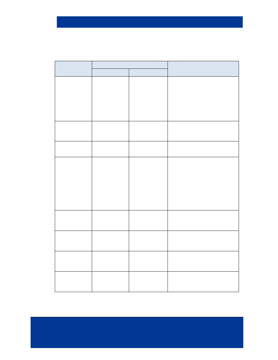
Table 5-5: P2 I/O Electrical Specifications
Pin Name
Parameters
Notes
Voltage
Current
Supply Voltage
Positive (V+)
Supply Voltage
Negative (V-)
+4.0 VDC to
10.0 VDC
0VDC or Ground
+40mA nominal
+80mA max
40mA is Polling, 80mA is Reading.
The power supply current draw is
normalized from 4.0 to
10 VDC in. The Battery+ has
reverse voltage protection.
Note: If implementing the OEM75 in
a UL listed product, UL requires
voltage range tolerances
of -15% to +10%.
Wiegand Data0
0V to 3.3V (+/–
0.3V)
+3mADCmax
-25mADC max
The module has 3.3VDC regulation.
The Interface circuit is a NPN
transistor with a 1K Collector to a
3.3VDC rail.
Wiegand Data1
0V to 3.3V (+/–
0.3V)
+3mADCmax
-25mADC max
There is no protection against
reverse voltage or exceeding the
limits specified on Data 0/1.
/Reset
0V to 3.3V (+/–
0.3V)
+0.33mADC
-5mADC max
The minimum VDD rise time for the
processor is 0.050V/mS. There is an
internal 10K Pull up to a continuous
3.3VDC rail. For this reason the
/RESET is best left unconnected, if
not needed. The OEM may control
this by an open drain or collector
signal to control a reset or power-on
reset. Avoid leakage currents on this
signal. Low Active, TTL 0-3.3VDC
Input.
/Hold
0V to 3.3V (+/–
0.3V)
-0mA
+0.33mA nominal
Internal limit of 10K series to DTL
circuit, an internal diode blocks the
10V
in
max limit specified. Low Active
DTL 0-5 VDC input.
/Green LED and
Card Present
0V to 3.3V (+/–
0.3V)
+0mA
-25mADC max
To an Open Collector NPN
transistor; this signal does not
source current, nor voltage. Low
Active Open Collector.
/Beeper
0V to 3.3V (+/–
0.3V)
+0mA
-50mADC max
To an Open Collector NPN
transistor; this signal does not
source current, nor voltage. Low
Active Open Collector.
/Red LED
0V to 3.3V (+/–
0.3V)
+0mA
-25mADC max
To an Open Collector NPN
transistor; this signal does not
source current, nor voltage. Low
Active Open Collector.