2 clear cmos jumper (jp3), 3 lvds1 voltage selection jumper (jp4), 4 lvds2 voltage selection jumper (jp1) – IEI Integration ECW-281B_D2550 User Manual
Page 104: 5 lvds2 panel type selection switch (sw1), Table 6-27: clear cmos jumper (jp3) settings
ECW-281B-D2550 Embedded System
Page 90
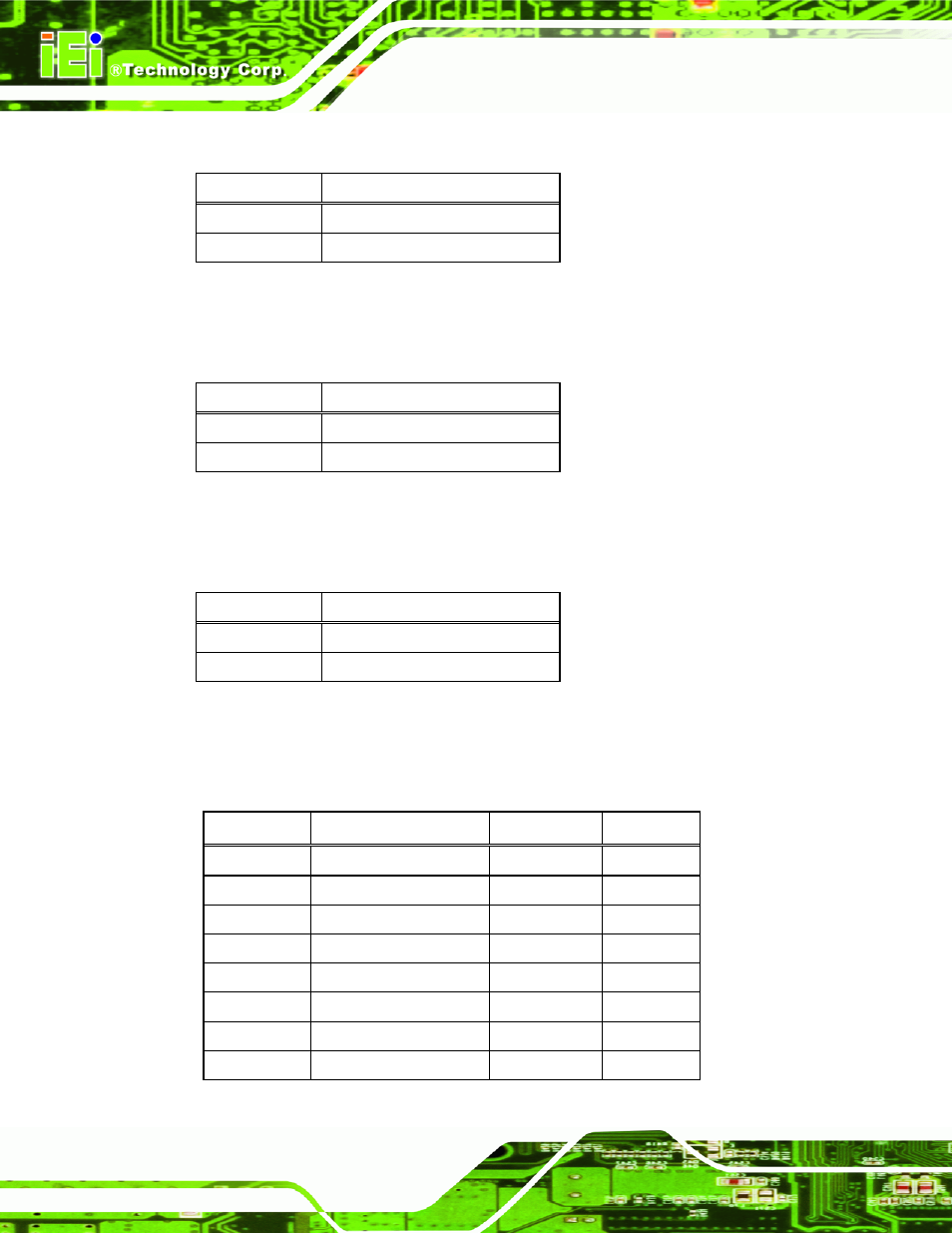
6.4.2 Clear CMOS Jumper (JP3)
Pin Description
Short 1-2
Keep CMOS Setup (Default)
Short 2-3
Clear CMOS Setup
Table 6-27: Clear CMOS Jumper (JP3) Settings
6.4.3 LVDS1 Voltage Selection Jumper (JP4)
Pin Description
Short 1-2
+3.3V LVDS (Default)
Short 2-3
+5V LVDS
Table 6-28: LVDS1 Voltage Selection Jumper (JP4) Settings
6.4.4 LVDS2 Voltage Selection Jumper (JP1)
Pin Description
Short 1-2
+3.3V LVDS (Default)
Short 2-3
+5V LVDS
Table 6-29: LVDS2 Voltage Selection Jumper (JP1) Settings
6.4.5 LVDS2 Panel Type Selection Switch (SW1)
Pin No.
4321
EDID Resolution
Color Depth
Channel
0000
800 x 600 @ 60 Hz
18-bit
Single
0001
1024 x 768 @ 60Hz
18-bit
Single
0010
1024 x 768 @ 60Hz
24-bit
Single
0011
1280 x 768 @ 60Hz
18-bit
Single
0100
1280 x 800 @ 60Hz
18-bit
Single
0101
1280 x 960 @ 60Hz
18-bit
Single
0110
1280 x 1024 @ 60Hz
24-bit
Dual
0111
1366 x 768 @ 60Hz
18-bit
Single