Rainbow Electronics MAX2769B User Manual
Max2769b universal gps receiver, Block diagram, General description
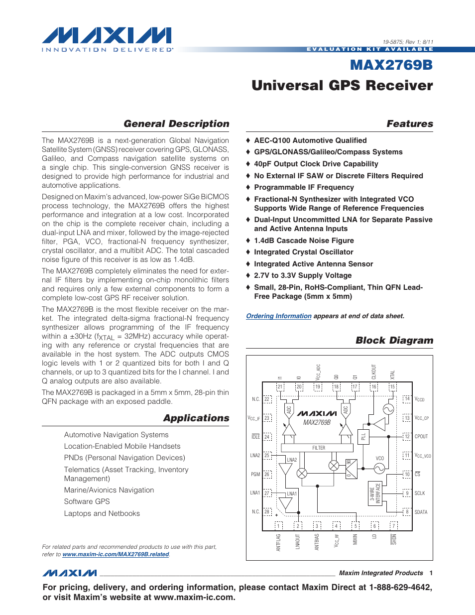
Table of contents
Document Outline
- General Description
- Applications
- Features
- Block Diagram
- Absolute Maximum Ratings
- DC Electrical Characteristics
- Typical Operating Characteristics
- Typical Operating Characteristics (continued)
- Typical Operating Characteristics (continued)
- Typical Application Circuit
- Pin Configuration
- Pin Description
- Detailed Description
- Integrated Active Antenna Sensor
- Low-Noise Amplifier (LNA)
- Mixer
- Programmable Gain Amplifier (PGA)
- Automatic Gain Control (AGC)
- Baseband Filter
- Synthesizer
- Crystal Oscillator
- ADC
- Fractional Clock Divider
- DSP Interface
- Preconfigured Device States
- Power-On Reset (POR)
- Serial Interface, Address, and Bit Assignments
- Detailed Register Definitions
- Applications Information
- Layout Issues
- Power-Supply Layout
- Chip Information
- Ordering Information
- Package Information
- Revision History
- LIST OF FIGURES
- LIST OF TABLES
- Table 1. Component List
- Table 2. Output Data Format
- Table 3. Preconfigured Device States
- Table 4. Serial-Interface Timing Require
- Table 5. Default Register Settings Overv
- Table 6. Default Register Settings
- Table 7. Configuration 1 (Address: 0000)
- Table 8. Configuration 2 (Address: 0001)
- Table 9. Configuration 3 (Address: 0010)
- Table 9. Configuration 3 (Address: 0010)
- Table 10. PLL Configuration (Address: 00
- Table 10. PLL Configuration (Address: 00
- Table 11. PLL Integer Division Ratio (Ad
- Table 12. PLL Division Ratio (Address 01
- Table 13. Reserved (Address 0110)
- Table 14. Clock Fractional Division Rati
- Table 15. Test Mode 1 (Address 1000)
- Table 16. Test Mode 2 (Address 1001)