Applications information, Layout issues, Power-supply layout – Rainbow Electronics MAX2769B User Manual
Page 23: Table 14. clock fractional division rati, Table 15. test mode 1 (address 1000), Table 16. test mode 2 (address 1001), Max2769b universal gps receiver
���������������������������������������������������������������� Maxim Integrated Products 23
MAX2769B
Universal GPS Receiver
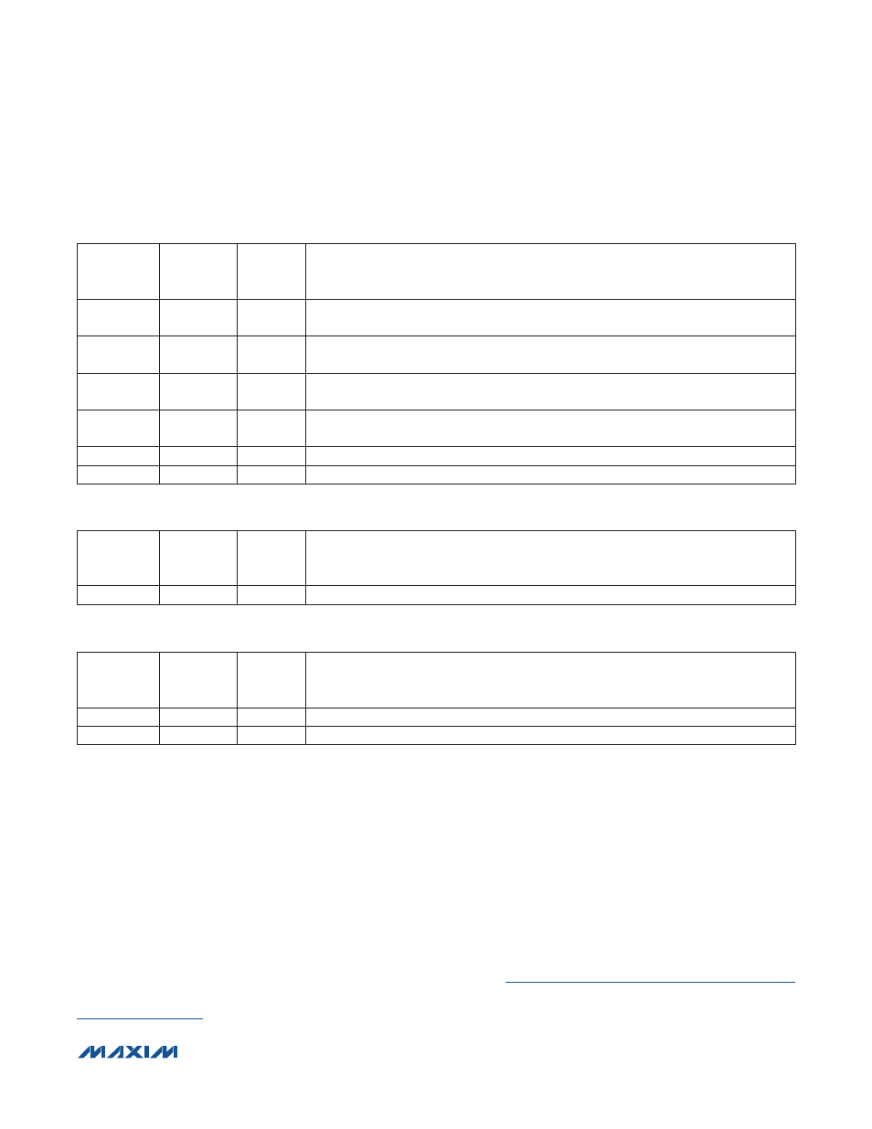
Table 14. Clock Fractional Division Ratio (Address 0111)
Table 15. Test Mode 1 (Address 1000)
Table 16. Test Mode 2 (Address 1001)
Applications Information
The LNA and mixer inputs require careful consideration
in matching to 50I lines. Proper supply bypassing,
grounding, and layout are required for reliable perfor-
mance from any RF circuit.
Layout Issues
The MAX2769B EV kit can be used as a starting point
for layout. For best performance, take into consideration
grounding and routing of RF, baseband, and power-
supply PCB proper line. Make connections from vias
to the ground plane as short as possible. On the high-
impedance ports, keep traces short to minimize shunt
capacitance. EV kit Gerber files can be requested at
Power-Supply Layout
To minimize coupling between different sections of the
IC, a star power-supply routing configuration with a large
decoupling capacitor at a central V
CC_
node is recom-
mended. The V
CC_
traces branch out from this node,
each going to a separate V
CC_
node in the circuit. Place
a bypass capacitor as close as possible to each supply
pin This arrangement provides local decoupling at each
V
CC_
pin. Use at least one via per bypass capacitor for
a low-inductance ground connection. Do not share the
capacitor ground vias with any other branch.
Refer to
for more information.
DATA BIT
LOCATION
DEFAULT
VALUE
(PGM = 0)
DESCRIPTION
L_CNT
27:16
256d
Sets the value for the L counter. 000100000000 = 256 fractional clock divider,
100000000000 = 2048 fractional clock divider.
M_CNT
15:4
1563d
Sets the value for the M counter. 011000011011 = 1563 fractional clock divider,
100000000 = 2048 fractional clock divider.
FCLKIN
3
0
Fractional clock divider. Set 1 to select the ADC clock to come from the fractional clock
divider, or 0 to bypass the ADC clock from the fractional clock divider.
ADCCLK
2
0
ADC clock selection. Set 0 to select the ADC and fractional divider clocks to come from
the reference divider/multiplier.
RESERVED
1
1
—
MODE
0
0
DSP interface mode selection.
DATA BIT
LOCATION
DEFAULT
VALUE
(PGM = 0)
DESCRIPTION
RESERVED
27:0
1E0F401
—
DATA BIT
LOCATION
DEFAULT
VALUE
(PGM = 0)
DESCRIPTION
RESERVED
27:1
28C0402 —
FCENMSB
0
0
When combined with FCEN, this bit represents the MSB of a 7-bit FCEN word.