Pin configuration, Pin description, Max2769b universal gps receiver – Rainbow Electronics MAX2769B User Manual
Page 11: Pin description pin configuration
���������������������������������������������������������������� Maxim Integrated Products 11
MAX2769B
Universal GPS Receiver
Pin Description
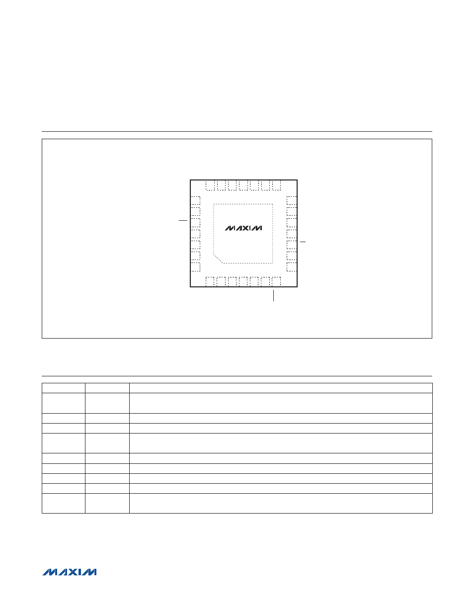
Pin Configuration
PIN
NAME
FUNCTION
1
ANTFLAG
Active Antenna Flag Logic Output. A logic-high indicates that an active antenna is connected to the
ANTBIAS pin.
2
LNAOUT
LNA Output. The LNA output is internally matched to 50I.
3
ANTBIAS
Buffered Supply Voltage Output. Provides a supply voltage bias for an external active antenna.
4
V
CC_RF
RF Section Supply Voltage. Bypass to ground with 100nF and 100pF capacitors in parallel as close
as possible to the pin.
5
MIXIN
Mixer Input. The mixer input is internally matched to 50I.
6
LD
Lock-Detector CMOS Logic Output. A logic-high indicates the PLL is locked.
7
SHDN
Operation Control Logic Input. A logic-low shuts off the entire device.
8
SDATA
Data Digital Input of 3-Wire Serial Interface
9
SCLK
Clock Digital Input of 3-Wire Serial Interface. Active when CS is low. Data is clocked in on the rising
edge of the SCLK.
MAX2769B
TQFN
TOP VIEW
26
27
25
24
10
9
11
LNAOUT
V
CC_RF
MIXIN
LD
12
ANTFLAG
I0
Q0
Q1
I1
CLKOUT
XTAL
1
2
LNA2
4
5
6
7
20
21
19
17
16 15
PGM
LNA1
CPOUT
V
CC_VCO
SCLK
ANTBIAS
V
CC_ADC
3
18
28
8
N.C.
EP
SDATA
+
23
13 V
CC_CP
V
CC_IF
22
14 V
CCD
N.C.
SHDN
CS
IDLE