Preconfigured device states, Power-on reset (por), Serial interface, address, and bit assignments – Rainbow Electronics MAX2769B User Manual
Page 17: Figure 4. v power-on reset, Table 3. preconfigured device states, Max2769b universal gps receiver
���������������������������������������������������������������� Maxim Integrated Products 17
MAX2769B
Universal GPS Receiver
Preconfigured Device States
When a serial interface is not available, the device can
be used in preconfigured states that don’t require pro-
gramming through the serial interface. Connecting the
PGM pin to logic-high and SCLK, SDATA, and CS pins
to either logic-high or low sets the device in one of the
preconfigured states according to
.
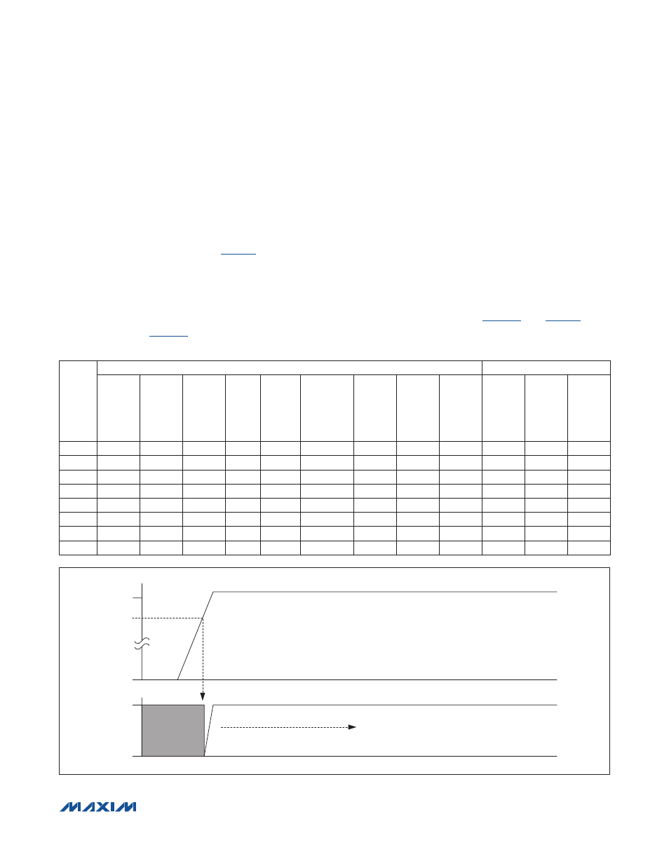
Power-On Reset (POR)
The MAX2769B incorporates power-on reset circuitry to
ensure that register settings are loaded upon power-up.
To ensure proper operation, the rising edge of PGM must
occur no sooner than when V
CC_
reaches 90% of its final
nominal value; see
Serial Interface, Address, and
Bit Assignments
A serial interface is used to program the MAX2769B for
configuring the different operating modes.
The serial interface is controlled by three signals: SCLK
(serial clock), CS (chip select), and SDATA (serial data).
The control of the PLL, AGC, test, and block selection
is performed through the serial-interface bus from the
baseband controller. A 32-bit word, with the MSB (D27)
being sent first, is clocked into a serial shift register when
the chip-select signal is asserted low. The timing of the
interface signals is shown in
with typical values for setup and hold time requirements.
Table 3. Preconfigured Device States
Figure 4. V
CC_
Power-On Reset
DEVICE STATE
DEVICE ELECTRICAL CHARACTERISTICS
3-WIRE CONTROL PINS
REFERENCE
FREQUENCY
(MHz)
REFERENCE
DIVISION
RATIO
MAIN
DIVISION
RATIO
I AND Q OR I
ONLY
NUMBER OF
IQ BITS
I AND Q
LOGIC LEVEL
IF CENTER
FREQUENCY
(MHz)
IF FILTER
BW (MHz)
IF FILTER
ORDER
SCLK
DATA
CS
0
16.368
16
1536
I
1
Differential
4.092
2.5
5th
0
0
0
1
16.368
16
1536
I
1
Differential
4.092
2.5
3rd
0
0
1
2
16.368
16
1536
I
2
CMOS
4.092
2.5
5th
0
1
0
3
32.736
32
1536
I
2
CMOS
4.092
2.5
5th
0
1
1
4
19.2
96
7857
I
2
CMOS
4.092
2.5
5th
1
0
0
5
27.456
26
1488
I
3
CMOS
4.092
4.2
5th
1
0
1
6
16.368
16
1536
I
3
CMOS
4.092
4.2
5th
1
1
0
7
27.456
26
1508
I
3
CMOS
9.27075
9.66
5th
1
1
1
90%
TIME (s)
TIME (s)
PGM = 0
PGM
PGM RISING EDGE ANYTIME
AFTER V
CC_
HAS REACHED
90% OF ITS NOMINAL VALUE.
0%
V
CC_
100%