Max2769b universal gps receiver, Ac electrical characteristics* (continued) – Rainbow Electronics MAX2769B User Manual
Page 4
����������������������������������������������������������������� Maxim Integrated Products 4
MAX2769B
Universal GPS Receiver
AC ELECTRICAL CHARACTERISTICS* (continued)
(MAX2769B EV kit, V
CC_
= 2.7V to 3.3V, T
A
= -40NC to +85NC, PGM = Ground. Registers are set to the default power-up states. LNA
input is driven from a 50I source. All RF measurements are done in the analog output mode with ADC bypassed. PGA gain is set
to 51dB gain by serial-interface word GAININ = 111010. Maximum IF output load is not to exceed 10kI||7.5pF on each pin. Typical
values are at V
CC_
= 2.85V and T
A
= +25NC, unless otherwise noted.) (Note 1)
Note 1: MAX2769B is production tested at T
A
= +25NC and +85NC. All min/max specifications are guaranteed by design and char-
acterization from -40NC to +85NC, unless otherwise noted. Default register settings are not production tested or guaran-
teed. User must program the registers upon power-up.
Note 2: Default, low-NF mode of the IC. LNA choice is gated by the ANT_FLAG signal. In the normal mode of operation without an
active antenna, LNA1 is active. If an active antenna is connected and ANT_FLAG switches to 1, LNA1 is automatically dis-
abled and LNA2 becomes active. PLL is in an integer-N mode with f
COMP
= f
TCXO
/16 = 1.023MHz and ICP = 0.5mA. The
complex IF filter is configured as a 5th-order Butterworth filter with a center frequency of 4MHz and bandwidth of 2.5MHz.
Output data is in a 2-bit sign/magnitude format at CMOS logic levels in the I channel only.
Note 3: The LNA output connects to the mixer input without a SAW filter between them.
Note 4: Two tones are located at 12MHz and 24MHz offset frequencies from the GPS center frequency of 1575.42MHz at -60dBm/
tone. Passive pole at the mixer output is programmed to be 13MHz.
Note 5: Measured from the LNA input to the LNA output. Two tones are located at 12MHz and 24MHz offset frequencies from the
GPS center frequency of 1575.42MHz at -60dBm per tone.
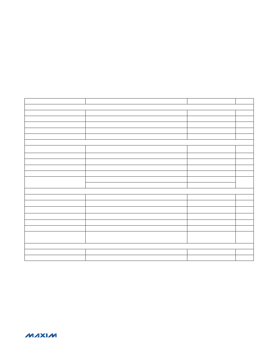
PARAMETER
CONDITIONS
MIN
TYP
MAX
UNITS
LNA2 INPUT
Power Gain
13
dB
Noise Figure
1.14
dB
Input IP3
(Note 5)
1
dBm
Output Return Loss
19
dB
Input Return Loss
11
dB
FREQUENCY SYNTHESIZER
LO Frequency Range
0.2V < V
TUNE
< (V
CC_
- 0.3V)
1550
1610
MHz
LO Tuning Gain
57
MHz/V
Reference Input Frequency
8
44
MHz
Main Divider Ratio
36
32,767
—
Reference Divider Ratio
1
1023
—
Charge-Pump Current
ICP = 0
0.5
mA
ICP = 1
1
TCXO INPUT BUFFER/OUTPUT CLOCK BUFFER
Frequency Range
8
32
MHz
Output Logic-Level High (V
OH
)
With respect to ground, I
OH
= 10FA (DC-coupled)
2
V
Output Logic-Level Low (V
OL
)
With respect to ground, I
OL
= 10FA (DC-coupled)
0.8
V
Capacitive Slew Current
Load = 10k
W + 40pF, f
CLKOUT
= 32MHz
11
mA
Output Load
10||40
kI||pF
Reference Input Level
Sine wave
0.5
V
P-P
Clock Output Multiply/Divide
Range
/4, /2, /1
(x2, max input frequency of 16MHz)
÷4
x2
—
ADC
ADC Differential Nonlinearity
AGC enabled, 3-bit output
Q
0.1
LSB
ADC Integral Nonlinearity
AGC enabled, 3-bit output
Q
0.1
LSB
*The parametric values (min, typ, max limits) shown in the Electrical Characteristics table supersede values quoted elsewhere in this data sheet.