Rainbow Electronics MAX2769B User Manual
Max2769b universal gps receiver, Block diagram, General description
MAX2769B
Universal GPS Receiver
����������������������������������������������������������������� Maxim Integrated Products 1
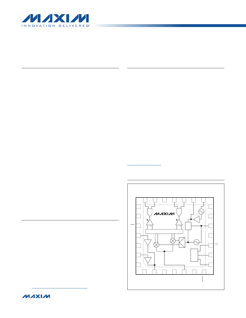
Block Diagram
19-5875; Rev 1; 8/11
For related parts and recommended products to use with this part,
refer to
www.maxim-ic.com/MAX2769B.related
.
E V A L U A T I O N K I T A V A I L A B L E
General Description
The MAX2769B is a next-generation Global Navigation
Satellite System (GNSS) receiver covering GPS, GLONASS,
Galileo, and Compass navigation satellite systems on
a single chip. This single-conversion GNSS receiver is
designed to provide high performance for industrial and
automotive applications.
Designed on Maxim’s advanced, low-power SiGe BiCMOS
process technology, the MAX2769B offers the highest
performance and integration at a low cost. Incorporated
on the chip is the complete receiver chain, including a
dual-input LNA and mixer, followed by the image-rejected
filter, PGA, VCO, fractional-N frequency synthesizer,
crystal oscillator, and a multibit ADC. The total cascaded
noise figure of this receiver is as low as 1.4dB.
The MAX2769B completely eliminates the need for exter-
nal IF filters by implementing on-chip monolithic filters
and requires only a few external components to form a
com plete low-cost GPS RF receiver solution.
The MAX2769B is the most flexible receiver on the mar-
ket. The integrated delta-sigma fractional-N frequency
synthesizer allows programming of the IF frequency
within a ±30Hz (f
XTAL
= 32MHz) accuracy while operat-
ing with any reference or crystal frequencies that are
available in the host system. The ADC outputs CMOS
logic levels with 1 or 2 quantized bits for both I and Q
channels, or up to 3 quantized bits for the I channel. I and
Q analog outputs are also available.
The MAX2769B is packaged in a 5mm x 5mm, 28-pin thin
QFN package with an exposed paddle.
Applications
Automotive Navigation Systems
Location-Enabled Mobile Handsets
PNDs (Personal Navigation Devices)
Telematics (Asset Tracking, Inventory
Management)
Marine/Avionics Navigation
Software GPS
Laptops and Netbooks
Features
S
AEC-Q100 Automotive Qualified
S
GPS/GLONASS/Galileo/Compass Systems
S
40pF Output Clock Drive Capability
S
No External IF SAW or Discrete Filters Required
S
Programmable IF Frequency
S
Fractional-N Synthesizer with Integrated VCO
Supports Wide Range of Reference Frequencies
S
Dual-Input Uncommitted LNA for Separate Passive
and Active Antenna Inputs
S
1.4dB Cascade Noise Figure
S
Integrated Crystal Oscillator
S
Integrated Active Antenna Sensor
S
2.7V to 3.3V Supply Voltage
S
Small, 28-Pin, RoHS-Compliant, Thin QFN Lead-
Free Package (5mm x 5mm)
LNAOUT
V
CC_RF
MIXIN
LD
ANTFLAG
I0
Q0
Q1
I1
CLKOUT
XTAL
LNA2
PGM
LNA1
CPOUT
V
CC_VCO
SCLK
ANTBIAS
V
CC_ADC
12
10
9
24
26
11
25
27
N.C.
SDATA
8
28
+
V
CC_CP
13
23
V
CC_IF
14 V
CCD
22
19
17
16
3
5
18
4
6
15
7
20
2
21
1
N.C.
SHDN
CS
ADC
ADC
FILTER
PLL
LNA2
LNA1
VCO
90
0
3-WIRE
INTERFACE
IDLE
MAX2769B
For pricing, delivery, and ordering information, please contact Maxim Direct at 1-888-629-4642,
or visit Maxim’s website at www.maxim-ic.com.
Document Outline
- General Description
- Applications
- Features
- Block Diagram
- Absolute Maximum Ratings
- DC Electrical Characteristics
- Typical Operating Characteristics
- Typical Operating Characteristics (continued)
- Typical Operating Characteristics (continued)
- Typical Application Circuit
- Pin Configuration
- Pin Description
- Detailed Description
- Integrated Active Antenna Sensor
- Low-Noise Amplifier (LNA)
- Mixer
- Programmable Gain Amplifier (PGA)
- Automatic Gain Control (AGC)
- Baseband Filter
- Synthesizer
- Crystal Oscillator
- ADC
- Fractional Clock Divider
- DSP Interface
- Preconfigured Device States
- Power-On Reset (POR)
- Serial Interface, Address, and Bit Assignments
- Detailed Register Definitions
- Applications Information
- Layout Issues
- Power-Supply Layout
- Chip Information
- Ordering Information
- Package Information
- Revision History
- LIST OF FIGURES
- LIST OF TABLES
- Table 1. Component List
- Table 2. Output Data Format
- Table 3. Preconfigured Device States
- Table 4. Serial-Interface Timing Require
- Table 5. Default Register Settings Overv
- Table 6. Default Register Settings
- Table 7. Configuration 1 (Address: 0000)
- Table 8. Configuration 2 (Address: 0001)
- Table 9. Configuration 3 (Address: 0010)
- Table 9. Configuration 3 (Address: 0010)
- Table 10. PLL Configuration (Address: 00
- Table 10. PLL Configuration (Address: 00
- Table 11. PLL Integer Division Ratio (Ad
- Table 12. PLL Division Ratio (Address 01
- Table 13. Reserved (Address 0110)
- Table 14. Clock Fractional Division Rati
- Table 15. Test Mode 1 (Address 1000)
- Table 16. Test Mode 2 (Address 1001)