Dsp interface, Figure 3. dsp interface top-level connec, Max2769b universal gps receiver – Rainbow Electronics MAX2769B User Manual
Page 16
���������������������������������������������������������������� Maxim Integrated Products 16
MAX2769B
Universal GPS Receiver
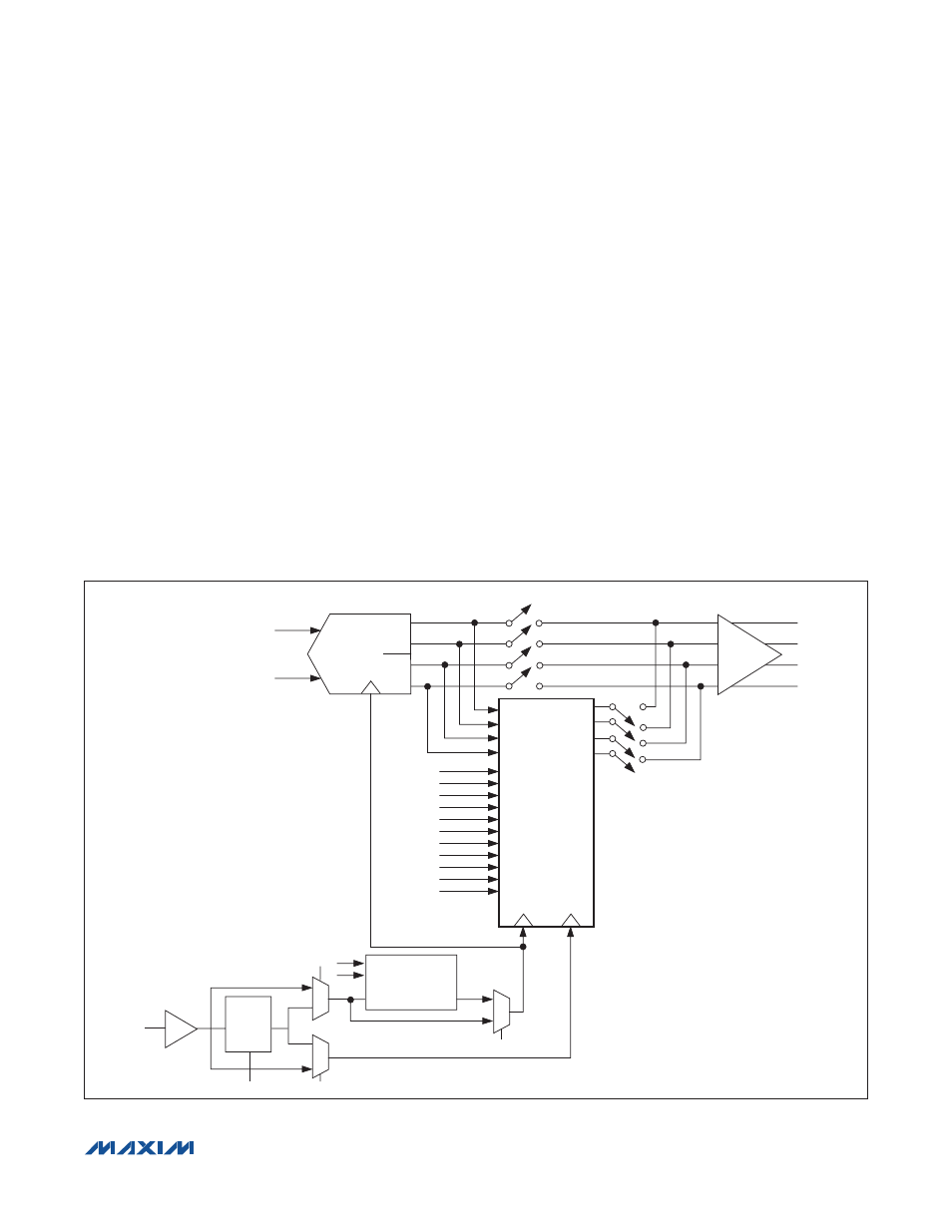
DSP Interface
GPS data is output from the ADC as the four logic sig nals
(bit
0
, bit
1
, bit
2
, and bit
3
) that represent sign/magnitude,
unsigned binary, or two’s complement binary data in
the I (bit
0
and bit
1
) and Q (bit
2
and bit
3
) channels. The
resolution of the ADC can be set up to 3 bits per channel.
For example, the 2-bit I and Q data in sign/magnitude
format is mapped as follows: bit
0
= I
SIGN
, bit
1
= I
MAG
,
bit
2
= Q
SIGN
, and bit
3
= Q
MAG
. The data can be serial-
ized in 16-bit segments of bit
0
, followed by bit
1
, bit
2
, and
bit
3
. The number of bits to be serialized is controlled by
the bits STRMBITS in the Configuration 3 register. This
selects between bit
0
; bit
0
and bit
1
; bit
0
and bit
2
; and
bit
0
, bit
1
, bit
2
, and bit
3
cases. If only bit
0
is serialized, the
data stream consists of bit
0
data only. If a serialization of
bit
0
and bit
1
(or bit
2
) is selected, the stream data pattern
consists of 16 bits of bit
0
data followed by 16 bits of bit
1
(or bit
2
) data, which, in turn, is followed by 16 bits of bit
0
data, and so on. In this case, the serial clock must be at
least twice as fast as the ADC clock. If a 4-bit serialization
of bit
0
, bit
1
, bit
2
, and bit
3
is chosen, the serial clock must
be at least four times faster than the ADC clock.
The ADC data is loaded in parallel into four holding
registers that correspond to four ADC outputs. Holding
registers are 16 bits long and are clocked by the ADC
clock. At the end of the 16-bit ADC cycle, the data is
transferred into four shift registers and shifted serially to
the output during the next 16-bit ADC cycle. Shift regis-
ters are clocked by a serial clock that must be chosen
fast enough so that all data is shifted out before the next
set of data is loaded from the ADC. An all-zero pattern
follows the data after all valid ADC data are streamed
to the output. A DATASYNC signal is used to signal the
beginning of each valid 16-bit data slice. In addition,
there is a TIME_SYNC signal that is output every 128 to
16,384 cycles of the ADC clock.
Figure 3. DSP Interface Top-Level Connectivity and Control Signals
STRM_EN
STRM_START
STRM_STOP
STRM_COUNT<2:0>
DIEID<1:0>
STRM_BITS<1:0>
FRM_COUNT<27:0>
STAMP_EN
DAT_SYNCEN
TIME_SYNCEN
STRM_RST
L_CNT<11:0>
M_CNT<11:0>
REFDIV<1:0>
BIT 0
PIN 21
PIN 20
PIN 17
PIN 18
BIT 1
BIT 2
BIT 3
DATA_OUT
CLK_SER
DATA_SYNC
TIME_SYNC
ADC
I
Q
CLK_ADC CLK_SER
CONTROL
SIGNALS
FROM 3-WIRE
INTERFACE
STRM_EN
OUTPUT
DRIVER
STRM_EN
CLK_IN
CLK_OUT
THROUGH
/2
/4
x2
REF/XTAL
PIN 15
ADCCLK_SEL
SERCLK_SEL
FRCLK_SEL