Figure 5. 3-wire timing diagram, Table 4. serial-interface timing require, Table 5. default register settings overv – Rainbow Electronics MAX2769B User Manual
Page 18: Figure 5, Table 4, Max2769b universal gps receiver
���������������������������������������������������������������� Maxim Integrated Products 18
MAX2769B
Universal GPS Receiver
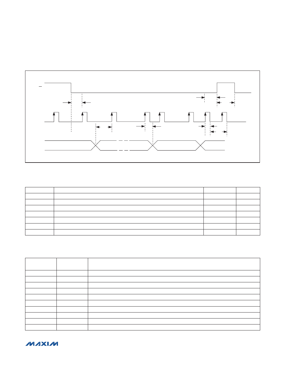
Figure 5. 3-Wire Timing Diagram
Table 4. Serial-Interface Timing Requirements
Table 5. Default Register Settings Overview
SYMBOL
PARAMETER
TYP VALUE
UNITS
t
CSS
Falling edge of CS to rising edge of the first SCLK time.
10
ns
t
DS
Data to serial-clock setup time.
10
ns
t
DH
Data to clock hold time.
10
ns
t
CH
Serial clock pulse-width high.
25
ns
t
CL
Clock pulse-width low.
25
ns
t
CSH
Last SCLK rising edge to rising edge of CS.
10
ns
t
CSW
CS high pulse width.
1
clock
REGISTER
NAME
ADDRESS
(A3:A0)
DATA
CONF1
0000
Configures RX and IF sections, bias settings for individual blocks.
CONF2
0001
Configures AGC and output sections.
CONF3
0010
Configures support and test functions for IF filter and AGC.
PLLCONF
0011
PLL, VCO, and CLK settings.
DIV
0100
PLL main and reference division ratios, other controls.
FDIV
0101
PLL fractional division ratio, other controls.
STRM
0110
DSP interface number of frames to stream.
CLK
0111
Fractional clock-divider values.
TEST1
1000
Reserved for test mode.
TEST2
1001
Reserved for test mode.
SCLK
CS
SDATA
DATA
MSB
DATA
LSB
ADDR
MSB
ADDR
LSB
t
CSH
t
CSW
t
CL
t
DH
t
CH
t
CSS
t
DS