Two wire interface and control registers, 1 two-wire interface (twi) protocol – Rainbow Electronics AT73C246 User Manual
Page 77
77
11050A–PMAAC–07-Apr-10
AT73C246
13. Two Wire Interface and Control Registers
13.1 Two-wire Interface (TWI) Protocol
The two-wire interface interconnects components on a unique two-wire bus, made up of one
clock line and one data line with speeds up to 400 Kbits per second, based one a byte oriented
transfer format. The TWI is slave only and single byte access.
The interface adds flexibility to the power supply solution, enabling LDO regulators to be con-
trolled depending on the instantaneous application requirements.
The AT73C246 has the following 7-bit address:1001001.
Attempting to read data from register addresses not listed in this section results in 0xFF being
read out.
• TWCK is an input pin for the clock
• TWD is an open-drain pin that drives or receives the serial data
The data put on the TWD line must be 8 bits long. Data is transferred MSB first. Each byte must
be followed by an acknowledgement.
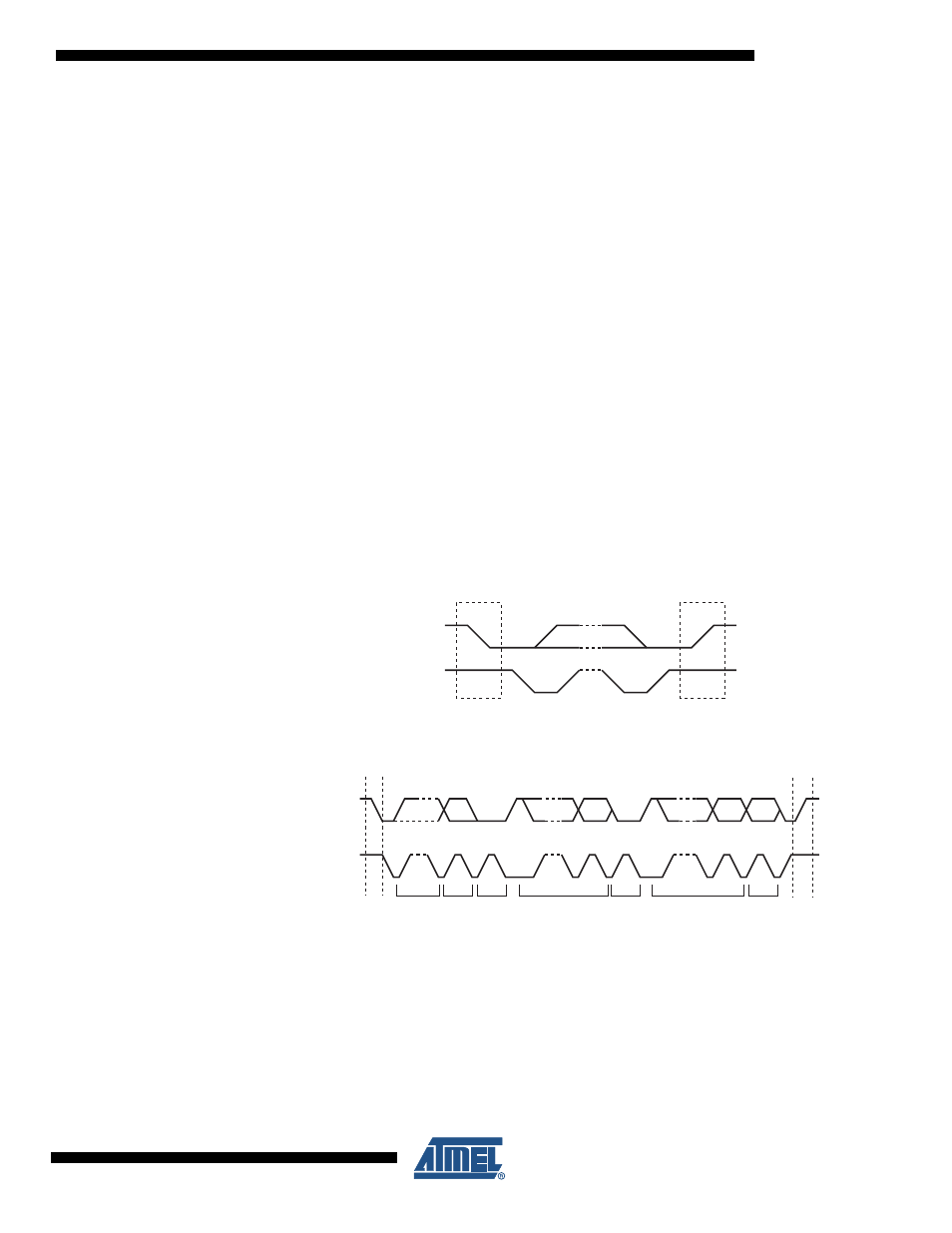
Each transfer begins with a START condition and terminates with a STOP condition.
• A high-to-low transition on TWD while TWCK is high defines a START condition.
• A low-to-high transition on TWD while TWCK is high defines a STOP condition.
Figure 13-1. TWI Start/Stop Cycle
Figure 13-2. TWI Data Cycle
After the host initiates a Start condition, it sends the 7-bit slave address defined above to notify
the slave device. A Read/Write bit follows (Read = 1, Write = 0).
The device acknowledges each received byte.
The first byte sent after device address and R/W bit is the address of the device register the host
wants to read or write.
For a write operation the data follows the internal address
TWD
TWCK
Start
Stop
TWD
TWCK
Start
Address
R/W
Ack
Data
Ack
Data
Ack
Stop