3 standby state, Sequence a sequence b, Is on. • vdd – Rainbow Electronics AT73C246 User Manual
Page 33: Symbol parameter comments min typ max units t
33
11050A–PMAAC–07-Apr-10
AT73C246
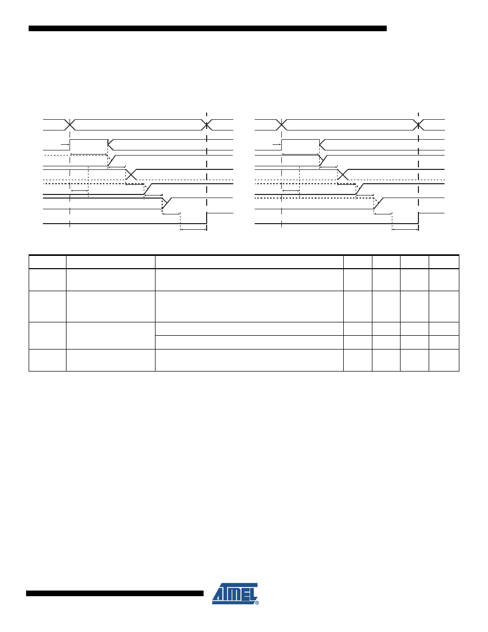
When RUN state is reached from the STANDBY state, the power supplies are sequentially
started-up according to the
Figure 11-6. AT73C246 - STANDBY to RUN state Supplies Start-Up timing diagram.
Note:
1. VDDx activity during STANDBY state is set by register PMU_STANDBY_SUPPLIES.
11.4.3
STANDBY STATE
When AT73C246 is in STANDBY state:
• V
BACKUP
is ON.
• VDD
{0,1,2,3}
are ON or OFF according to the status in register 0x03
(PMU_STANDBY_SUPPLIES)
• VDD
4
is ON or OFF according to the status in register 0x0A (VDD4_CTRL)
• Audio function is OFF
• ADC function is ON or OFF according to the status in register 0x30 (ADC_CTRL)
• RSTB pin is forced to ground.
• TWI pins are ignored to prevent TWI registers from corruption
• Led pin is driven according to register PMU_LED (0x0B)
To reach the STANDBY state, the appropriate power supplies are shut down as described in the
.
Table 11-5.
STANDBY to RUN state timing table
Symbol
Parameter
Comments
Min
Typ
Max
Units
T
ON_SYS
Start-up Time
Time from validated WAKEUP event (end of debounce
time when applicable) to VDD2 or VDD3 power on.
810
900
990
µs
T
PFM
PFM/PWM Switching
time
Time from validated WAKEUP event (end of debounce
time when applicable) to PFM/PWM switching if
applicable.
420
470
520
µs
T
ON_VDDx
VDDx Start-up Time
VDDx is OFF during STANDBY state
5.2
5.4
5.7
ms
VDDx is ON during STANDBY state
58
62
66
µs
T
RESET
All Regulators ON To
RSTB High
30.4
32
33.6
ms
SEQUENCE A
SEQUENCE B
STANDBY
STATE
SUPPLIES START UP
T
ON_SYS
RUN STATE
WAKEUP
EVENT
V
DD3
(3.3V)
T
ON_VDD3
T
ON_VDD0
T
ON_VDD1
V
DD2
(1V)
3.3V
1.85V
1.2V
1V
T
ON_VDD2
RSTB
VPAD LEVEL
T
RESET
V
DD3
ON
or OFF
STANDBY
STATE
SUPPLIES START UP
T
ON_SYS
RUN STATE
WAKEUP
EVENT
V
DD2
(1V)
T
ON_VDD2
T
ON_VDD0
T
ON_VDD1
V
DD3
(3.3V)
1V
1.85V
1.2V
3.3V
T
ON_VDD3
RSTB
VPAD LEVEL
T
RESET
V
DD3
ON
or OFF
V
DD0
(1.85V)
V
DD1
(1.2V)
PFM
T
PFM
PFM
V
DD0
(1.85V)
V
DD1
(1.2V)
PFM
T
PFM
PFM
PWM
V
DD0
PWM
V
DD1
PWM
V
DD0
PWM
V
DD1