4 hrst state, Sequence a sequence b, Symbol parameter comments min typ max units t – Rainbow Electronics AT73C246 User Manual
Page 34: Vddx shutdown time vddx is off during both stanby, An d run, Vddx is on during run state, Vddx startup time vddx is on during stanby st ate, Vddx is off during run state, And run
34
11050A–PMAAC–07-Apr-10
AT73C246
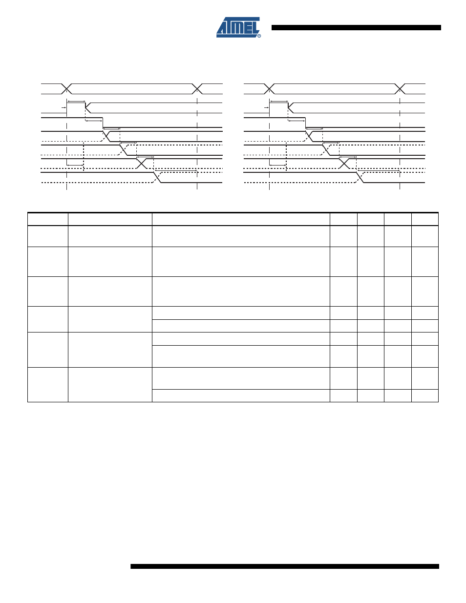
Figure 11-7. AT73C246 - RUN to STANDBY state Supplies Shutdown timing diagram.
Note:
1. VDDx activity during STANDBY state is set by register PMU_STANDBY_SUPPLIES.
2. VDDx activity during RUN state is set by Bit7 of register VDDx_CTRL.
11.4.4
HRST STATE
HRST state is a transition state used to restart the CPU:
• VDD
{0,1,2,3,4}
are switched off according to figure
depending on the
previous state
• VDD
5
is ON
• RSTB pin is forced to ground
Table 11-6.
RUN to STANDBY state timing table
Symbol
Parameter
Comments
Min
Typ
Max
Units
T
STANDBY
STANDBY Event
Detection Time
150
160
170
µs
T
PWM
PFM/PWM Switching
time
Time from validated WAKEUP event (end of debounce
time when applicable) to PFM/PWM switching if
applicable.
460
500
540
µs
T
WAIT
WAKEUP Event
Detection Window
If a WAKEUP event occurs in this window the PMU
automatically restart at the end of the STANDBY
process.
150
160
170
µs
T
OFF_AUDIO
Audio CODEC
Shutdown Time
Audio CODEC is ON
486
512
538
ms
Audio CODEC is OFF
58
62
66
µs
T
OFF_VDDx
VDDx SHUTDOWN
Time
VDDx is OFF during both STANBY
states.
58
62
66
µs
VDDx is OFF during STANBY state
.
VDDx is ON during RUN state
4.8
5.2
5.4
ms
T
ON_VDDx
VDDx STARTUP Time
VDDx is ON during STANBY state
.
VDDx is OFF during RUN state
4.8
5.2
5.4
ms
VDDx is ON during both STANBY
and RUN
states.
58
62
66
µs
RUN
STATE
SUPPLIES SHUTDOWN
STANDBY
EVENT
STANDBY
STATE
T
STANDBY
T
OFF_AUDIO
T
OFF_VDD2
T
WAIT +
V
DD2
(1V)
V
DD3
(3.3V)
1V
1.2V
1.85V
3.3V
RSTB
T
OFF_VDD1
T
OFF_VDD0
T
OFF_VDD3
1.85V
(
V
DD3
ON
or OFF
)
SEQUENCE A
SEQUENCE B
RUN
STATE
SUPPLIES SHUTDOWN
STANDBY
EVENT
STANDBY
STATE
T
STANDBY
T
OFF_AUDIO
T
OFF_VDD3
T
WAIT +
V
DD3
(3.3V)
V
DD2
(1V)
3.3V
1.2V
1.85V
1V
RSTB
T
OFF_VDD1
T
OFF_VDD0
T
OFF_VDD2
1.85V
(
V
DD3
ON
or OFF
)
V
DD1
(1.2V)
V
DD0
(1.85V)
T
PWM
PWM
PWM
V
DD1
(1.2V)
V
DD0
(1.85V)
T
PWM
PWM
PWM
PFM
V
DD0
PFM
V
DD1
PFM
V
DD0
PFM
V
DD1