In-system programmable flash program memory, Sram data memory, Attiny26(l) – Rainbow Electronics ATtiny26L User Manual
Page 9

9
ATtiny26(L)
1477B–AVR–04/02
In-System
Programmable Flash
Program Memory
The ATtiny26/L contains 2K bytes On-chip In-System Programmable Flash memory for
program storage. Since all instructions are 16- or 32-bit words, the Flash is organized as
1K x 16. The Flash memory has an endurance of at least 1,000 write/erase cycles. The
ATtiny26/L Program Counter – PC – is 10 bits wide, thus addressing the 1024 program
memory addresses, see “Memory Programming” on page 106 for a detailed description
on Flash data downloading. See “Program and Data Addressing Modes” on page 10 for
the different program memory addressing modes.
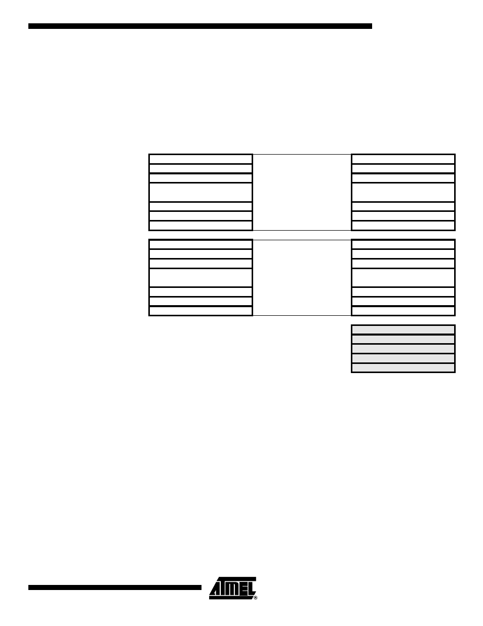
Figure 5. SRAM Organization
SRAM Data Memory
Figure 5 above shows how the ATtiny26/L SRAM Memory is organized.
The lower 224 Data Memory locations address the Register File, the I/O Memory and
the internal data SRAM. The first 96 locations address the Register File and I/O Mem-
ory, and the next 128 locations address the internal data SRAM.
The five different addressing modes for the data memory cover: Direct, Indirect with Dis-
placement, Indirect, Indirect with Pre-decrement, and Indirect with Post-increment. In
the Register File, registers R26 to R31 feature the indirect addressing pointer registers.
The direct addressing reaches the entire data space. The Indirect with Displacement
mode features a 63 address locations reach from the base address given by the Y- or Z-
register.
When using register indirect addressing modes with automatic pre-decrement and post-
increment, the address registers X, Y, and Z are decremented and incremented.
The 32 general purpose working registers, 64 I/O Registers and the 128 bytes of inter-
nal data SRAM in the ATtiny26/L are all accessible through all these addressing modes.
See the next section for a detailed description of the different addressing modes.
Register File
Data Address Space
R0
$0000
R1
$0001
R2
$0002
...
...
R29
$001D
R30
$001E
R31
$001F
I/O Registers
$00
$0020
$01
$0021
$02
$0022
…
…
$3D
$005D
$3E
$005E
$3F
$005F
Internal SRAM
$0060
$0061
...
$00DE
$00DF
