Timer/counter1 in pwm mode, Attiny26(l) – Rainbow Electronics ATtiny26L User Manual
Page 54

54
ATtiny26(L)
1477B–AVR–04/02
• Bit 1 – PLLE: PLL Enable
When the PLLE is set, the PLL is started and if needed internal RC Oscillator is started
as a PLL reference clock. If PLL is selected as a system clock source the value for this
bit is always 1.
• Bit 0 – PLOCK: PLL Lock Detector
When the PLOCK bit is set, the PLL is locked to the reference clock, and it is safe to
enable PCK for Timer/Counter1. After the PLL is enabled, it takes about 100 ms for the
PLL to lock.
Timer/Counter1 Initialization
for Asynchronous Mode
To change Timer/Counter1 to the asynchronous mode, first enable PLL, and poll the
PLOCK bit until it is set, and then set the PCKE bit.
Timer/Counter1 in PWM Mode
When the PWM mode is selected, Timer/Counter1 and the Output Compare Register C
– OCR1C form a dual 8-bit, free-running and glitch-free PWM generator with outputs on
the PB1(OC1A) and PB3(OC1B) pins. Also inverted, non-overlapping outputs are avail-
able on pins PB0(OC1A) and PB2(OC1B), respectively. The non-overlapping output
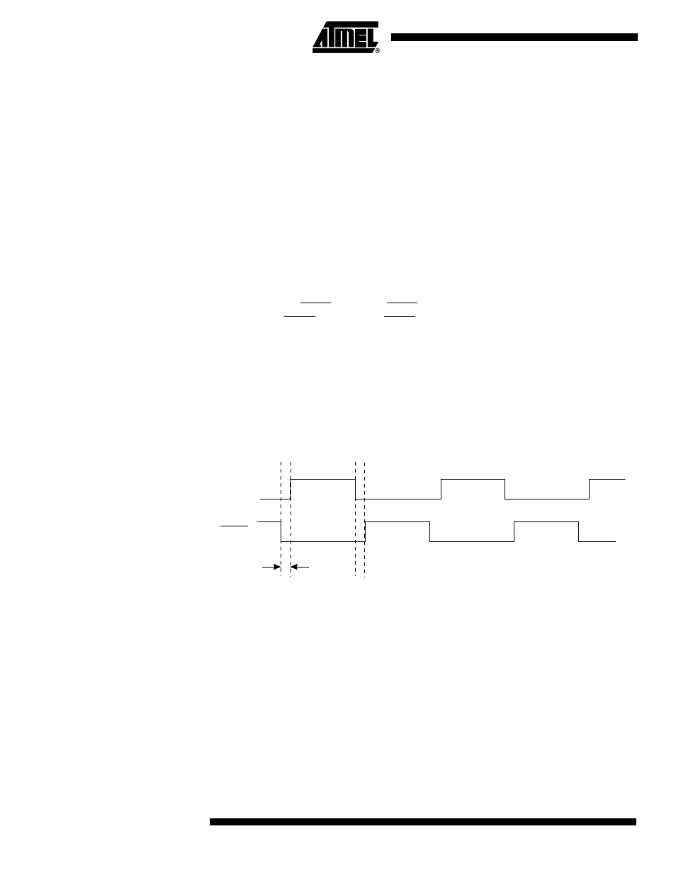
pairs (OC1A - OC1A and OC1B - OC1B) are never both set at the same time. This
allows driving power switches directly. The non-overlap time is one prescaled clock
cycle, and the high time is one cycle shorter than the low time.
The non-overlap time is generated by delaying the rising edge, i.e., the positive edge is
one prescaled and one PCK cycle delayed and the negative edge is one PCK cycle
delayed in the asynchronous mode. In the synchronous mode he positive edge is one
prescaled and one CK cycle delayed and the negative edge is one CK cycle delayed.
The high time is also one prescaled cycle shorter in the both operation modes.
Figure 36. The Non-overlapping Output Pair
When the counter value match the contents of OCR1A and OCR1B, the OC1A and
O C 1 B o u t p u t s a r e s e t o r c l e a r e d a c c o r d i n g t o t h e C O M 1 A 1 / C O M 1 A 0 o r
COM1B1/COM1B0 bits in the Timer/Counter1 Control Register A – TCCR1A, as shown
in Table 25 below.
Timer/Counter1 acts as an up-counter, counting from $00 up to the value specified in
the Output Compare Register (OCR1C), and starting from $00 up again. A compare
match with OC1C will set an Overflow Interrupt Flag (TOV1) after a synchronization
delay following the compare event.
OC1x
OC1x
x = A or B
t
non-overlap
