Timer/counter0 – tcnt0, Bit timer/counter1, Attiny26(l) – Rainbow Electronics ATtiny26L User Manual
Page 47
47
ATtiny26(L)
1477B–AVR–04/02
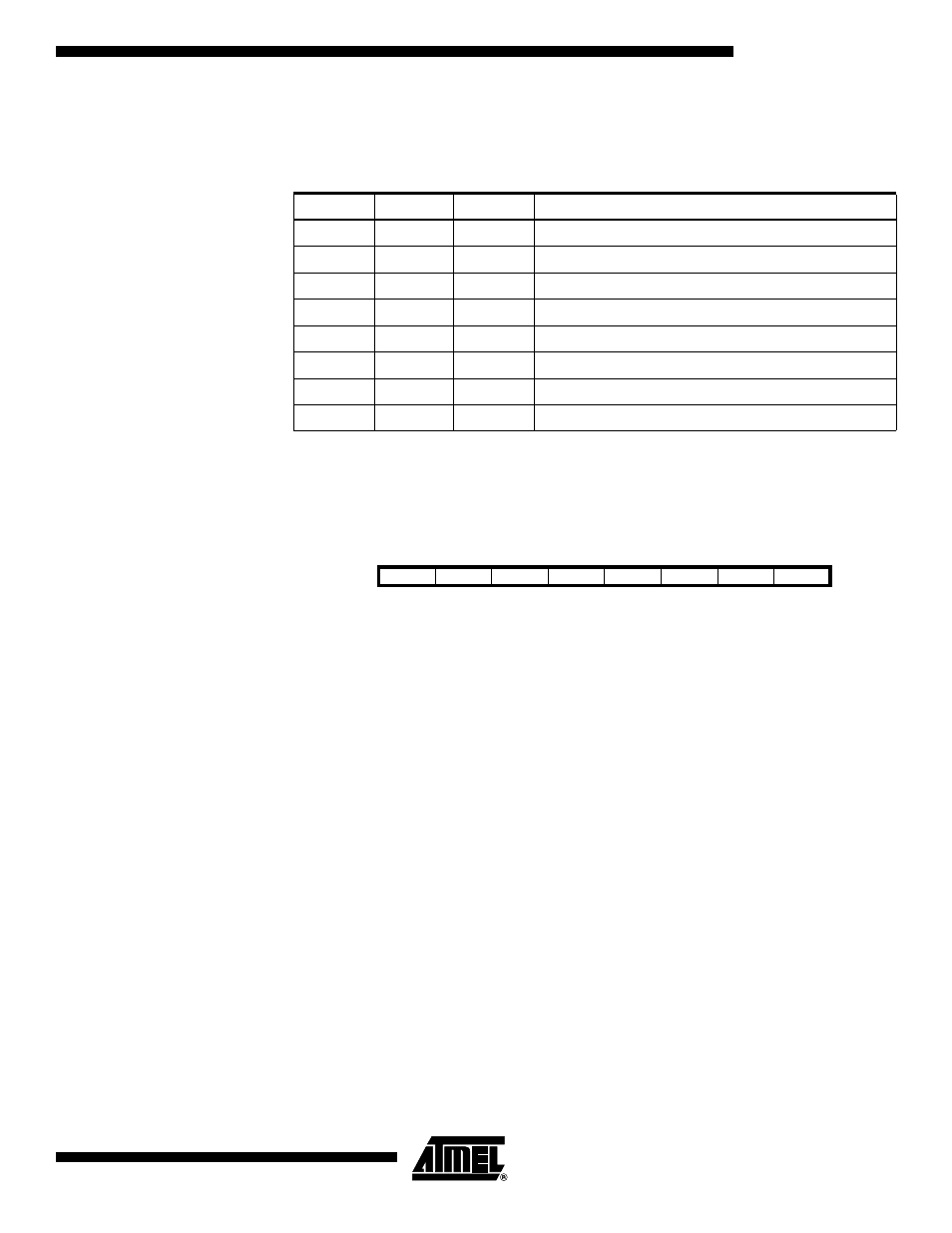
• Bits 2, 1, 0 – CS02, CS01, CS00: Clock Select0, Bit 2, 1, and 0
The Clock Select0 bits 2, 1, and 0 define the prescaling source of Timer0.
The Stop condition provides a Timer Enable/Disable function. The CK down divided
modes are scaled directly from the CK oscillator clock. If the external pin modes are
used, the corresponding setup must be performed in the actual Data Direction Control
Register (cleared to zero gives an input pin).
Timer/Counter0 – TCNT0
The Timer/Counter0 is implemented as an up-counter with read and write access. If the
Timer/Counter0 is written and a clock source is present, the Timer/Counter0 continues
counting in the timer clock cycle following the write operation.
8-bit Timer/Counter1
The Timer/Counter1 has two clocking modes: a synchronous mode and an asynchro-
nous mode. The synchronous mode uses the system clock (CK) as the clock timebase
and asynchronous mode uses the fast peripheral clock (PCK) as the clock time base.
The PCKE bit from the PLLCSR Register enables the asynchronous mode when it is set
(“1”). The Timer/Counter1 general operation is described in the asynchronous mode and
the operation in the synchronous mode is mentioned only if there is differences between
these two modes. Figure 34 shows Timer/Counter1 synchronization register block dia-
gram and synchronization delays in between registers. Note that all clock gating details
are not shown in the figure. The Timer/Counter1 Register values go through the internal
synchronization registers, which cause the input synchronization delay, before affecting
the counter operation. The registers TCCR1A, TCCR1B, OCR1A, OCR1B, and OCR1C
can be read back right after writing the register. The read back values are delayed for
the Timer/Counter1 (TCNT1) Register and flags (OCF1A, OCF1B, and TOV1), because
of the input and output synchronization.
This module features a high resolution and a high accuracy usage with the lower pres-
caling opportunities. Timer/Counter1 can also support two accurate, high speed, 8-bit
Pulse Width Modulators using clock speeds up to 64 MHz. In this mode, Timer/Counter1
and the Output Compare Registers serve as dual stand-alone PWMs with non-overlap-
ping non-inverted and inverted outputs. Refer to page 54 for a detailed description on
this function. Similarly, the high prescaling opportunities make this unit useful for lower
speed functions or exact timing functions with infrequent actions.
Table 21. Clock 0 Prescale Select
CS02
CS01
CS00
Description
0
0
0
Stop, the Timer/Counter0 is stopped
0
0
1
CK
0
1
0
CK/8
0
1
1
CK/64
1
0
0
CK/256
1
0
1
CK/1024
1
1
0
External Pin T0, falling edge
1
1
1
External Pin T0, rising edge
Bit
7
6
5
4
3
2
1
0
$32 ($52)
MSB
LSB
TCNT0
Read/Write
R/W
R/W
R/W
R/W
R/W
R/W
R/W
R/W
Initial Value
0
0
0
0
0
0
0
0