Prescaling and conversion timing, Attiny26(l) – Rainbow Electronics ATtiny26L User Manual
Page 79

79
ATtiny26(L)
1477B–AVR–04/02
minal, otherwise the gain stage will saturate at 0V (GND). This amplified value then
becomes the analog input to the ADC. If single ended channels are used, the gain
amplifier is bypassed altogether.
The ADC can operate in two modes – Single Conversion and Free Running mode. In
Single Conversion mode, each conversion will have to be initiated by the user. In Free
Running mode, the ADC is constantly sampling and updating the ADC Data Register.
The ADFR bit in ADCSR selects between the two available modes.
The ADC is enabled by setting the ADC Enable bit, ADEN in ADCSR. Voltage reference
and input channel selections will not go into effect until ADEN is set. The ADC does not
consume power when ADEN is cleared, so it is recommended to switch off the ADC
before entering power saving sleep modes.
A conversion is started by writing a logical one to the ADC Start Conversion bit, ADSC.
This bit stays high as long as the conversion is in progress and will be set to zero by
hardware when the conversion is completed. If a different data channel is selected while
a conversion is in progress, the ADC will finish the current conversion before performing
the channel change.
The ADC generates a 10-bit result, which is presented in the ADC Data Registers,
ADCH and ADCL. By default, the result is presented right adjusted, but can optionally
be presented left adjusted by setting the ADLAR bit in ADMUX.
If the result is left adjusted and no more than 8-bit precision is required, it is sufficient to
read ADCH. Otherwise, ADCL must be read first, then ADCH, to ensure that the content
of the data registers belongs to the same conversion. Once ADCL is read, ADC access
to data registers is blocked. This means that if ADCL has been read, and a conversion
completes before ADCH is read, neither register is updated and the result from the con-
version is lost. When ADCH is read, ADC access to the ADCH and ADCL Registers is
re-enabled.
The ADC has its own interrupt which can be triggered when a conversion completes.
When ADC access to the Data Registers is prohibited between reading of ADCH and
ADCL, the interrupt will trigger even if the result is lost.
Prescaling and
Conversion Timing
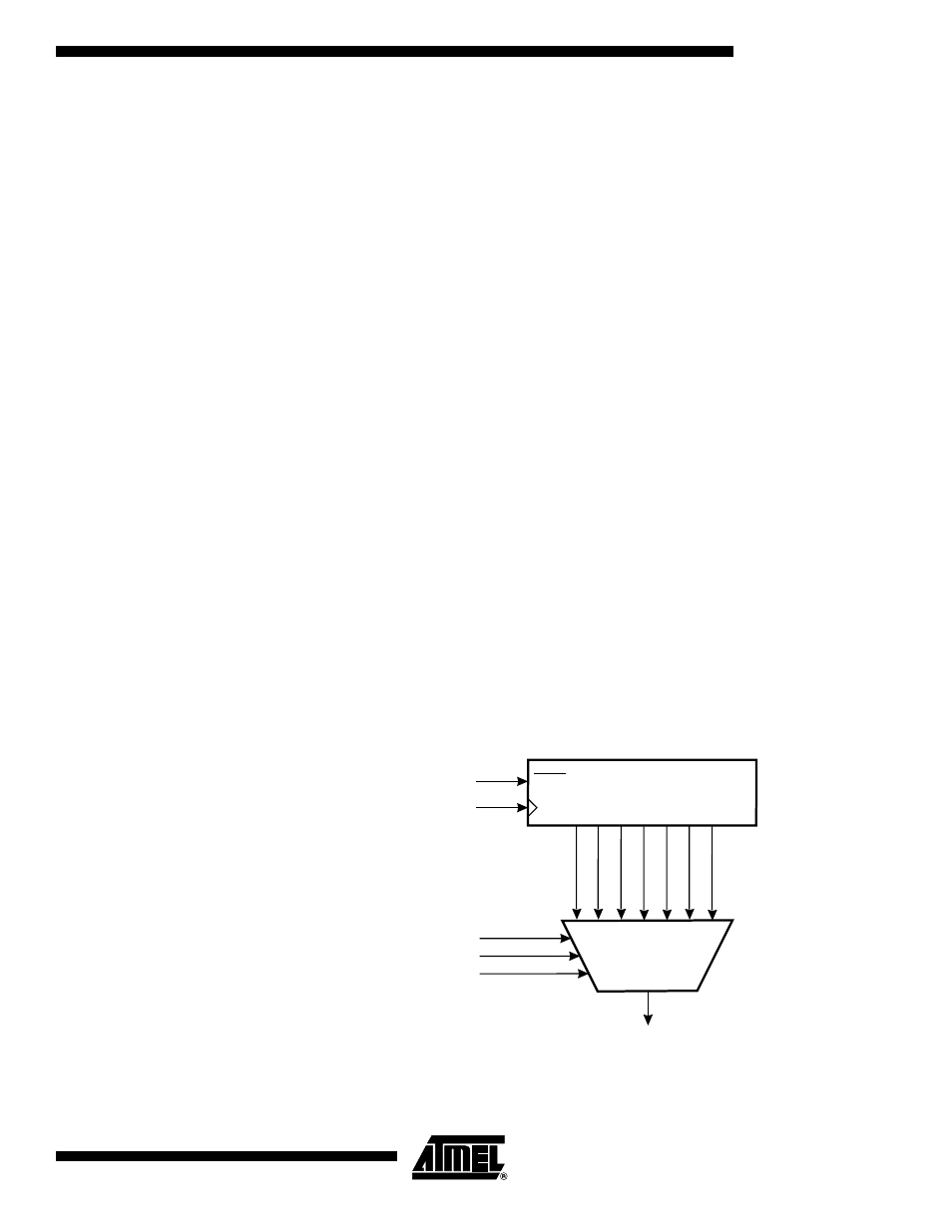
Figure 47. ADC Prescaler
7-BIT ADC PRESCALER
ADC CLOCK SOURCE
CK
ADPS0
ADPS1
ADPS2
CK/128
CK/2
CK/4
CK/8
CK/16
CK/32
CK/64
Reset
ADEN
