Attiny26(l) – Rainbow Electronics ATtiny26L User Manual
Page 80

80
ATtiny26(L)
1477B–AVR–04/02
The successive approximation circuitry requires an input clock frequency between
50 kHz and 200 kHz. The ADC module contains a prescaler, which divides the system
clock to an acceptable ADC clock frequency.
The ADPS bits in ADCSR are used to generate a proper ADC clock input frequency
from any chip clock frequency above 100 kHz. The prescaler starts counting from the
moment the ADC is switched on by setting the ADEN bit in ADCSR. The prescaler
keeps running for as long as the ADEN bit is set, and is continuously reset when ADEN
is low.
When initiating a conversion by setting the ADSC bit in ADCSR, the conversion starts at
the following rising edge of the ADC clock cycle. If differential channels are selected, the
conversion will only start at every other rising edge of the ADC clock cycle after ADEN
was set.
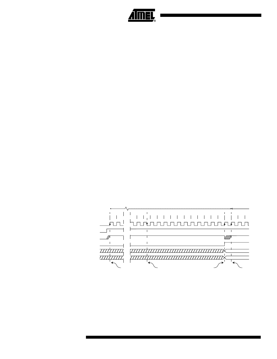
A normal conversion takes 13 ADC clock cycles. In certain situations, the ADC needs
more clock cycles to initialization and minimize offset errors. Extended conversions take
25 ADC clock cycles and occur as the first conversion after the ADC is switched on
(ADEN in ADCSR is set). Additionally, when changing voltage reference, the user may
improve accuracy by disregarding the first conversion result after the reference or MUX
setting was changed.
The actual sample-and-hold takes place 1.5 ADC clock cycles after the start of a normal
conversion and 13.5 ADC clock cycles after the start of an extended conversion. When
a conversion is complete, the result is written to the ADC Data Registers, and ADIF is
set. In Single Conversion mode, ADSC is cleared simultaneously. The software may
then set ADSC again, and a new conversion will be initiated on the first rising ADC clock
edge. In Free Running mode, a new conversion will be started immediately after the
conversion completes, while ADSC remains high. Using Free Running mode and an
ADC clock frequency of 200 kHz gives the lowest conversion time, 65
µs
, equivalent to
15 kSPS. For a summary of conversion times, see Table 34.
Figure 48. ADC Timing Diagram, Extended Conversion (Single Conversion Mode)
MSB of Result
LSB of Result
ADC Clock
ADSC
Sample & Hold
ADIF
ADCH
ADCL
Cycle Number
ADEN
1
2
12
13
14
15
16
17
18
19
20
21
22
23
24
25
1
2
Extended Conversion
Next
Conversion
3
MUX and REFS
Update
MUX and REFS
Update
Conversion
Complete
