Attiny26(l) – Rainbow Electronics ATtiny26L User Manual
Page 55

55
ATtiny26(L)
1477B–AVR–04/02
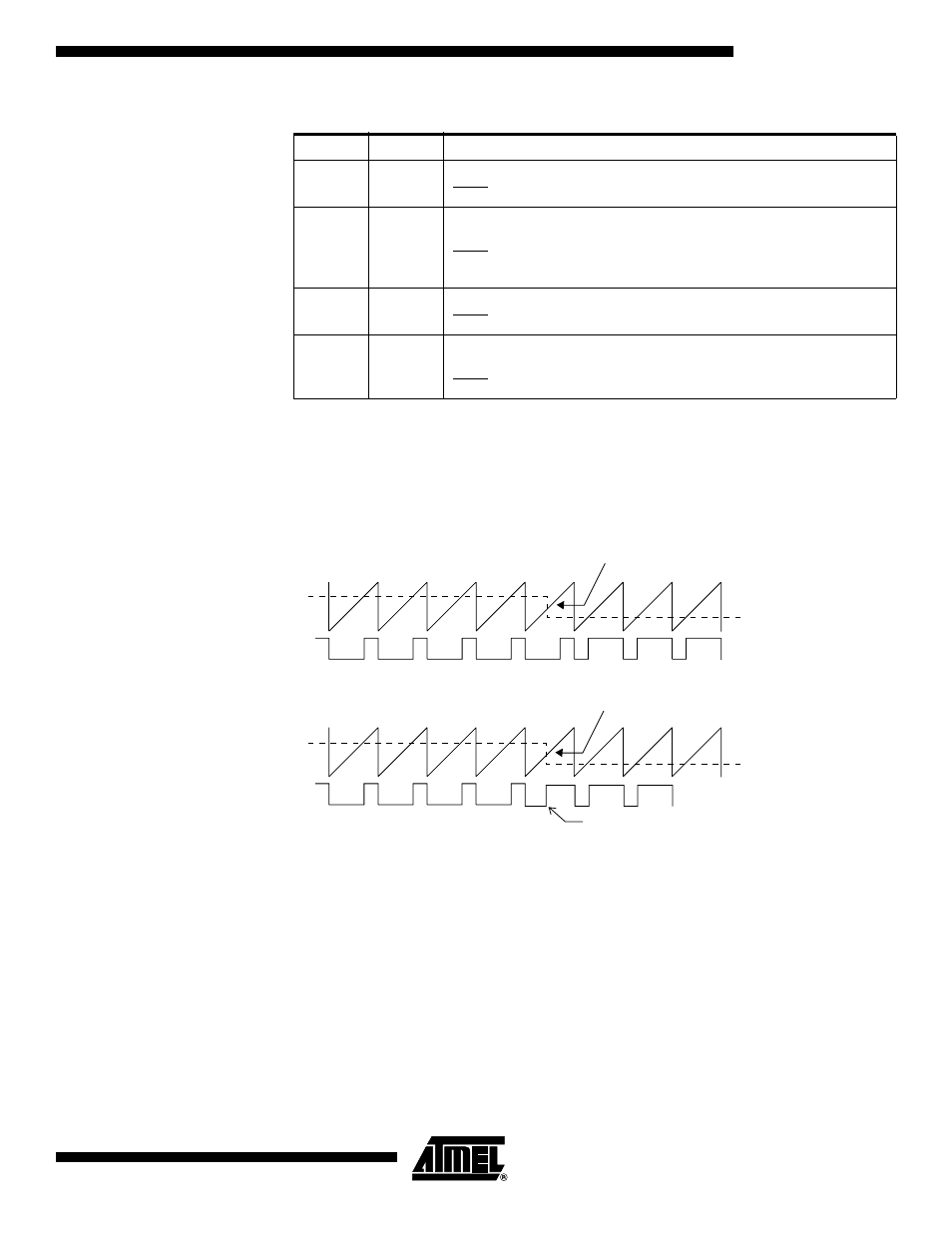
Note that in PWM mode, writing to the Output Compare Registers OCR1A or OCR1B,
the data value is first transferred to a temporary location. The value is latched into
OCR1A or OCR1B when the Timer/Counter reaches OCR1C. This prevents the occur-
rence of odd-length PWM pulses (glitches) in the event of an unsynchronized OCR1A or
OCR1B. See Figure 37 for an example.
Figure 37. Effects of Unsynchronized OCR Latching
During the time between the write and the latch operation, a read from OCR1A or
OCR1B will read the contents of the temporary location. This means that the most
recently written value always will read out of OCR1A or OCR1B.
When OCR1A or OCR1B contain $00 or the top value, as specified in OCR1C Register,
the output PB1(OC1A) or PB3(OC1B) is held low or high according to the settings of
COM1A1/COM1A0. This is shown in Table 26.
Table 25. Compare Mode Select in PWM Mode
COM1x1
COM1x0
Effect on Output Compare Pins
0
0
OC1x not connected.
OC1x not connected.
0
1
OC1x cleared on compare match. Set one prescaled cycle after
TCNT1 = $01.
OC1x set one prescaled cycle after compare match. Cleared when
TCNT1 = $00.
1
0
OC1x cleared on compare match. Set when TCNT1 = $01.
OC1x not connected.
1
1
OC1x set one prescaled cycle after compare match. Cleared when
TCNT = $00
OC1x not connected.
PWM Output OC1x
PWM Output OC1x
Unsynchronized OC1x Latch
Synchronized OC1x Latch
Counter Value
Compare Value
Counter Value
Compare Value
Compare Value changes
Glitch
Compare Value Changes
