P2conl – Samsung S3F80JB User Manual
Page 94
S3F80JB
CONTROL REGISTERS
4-27
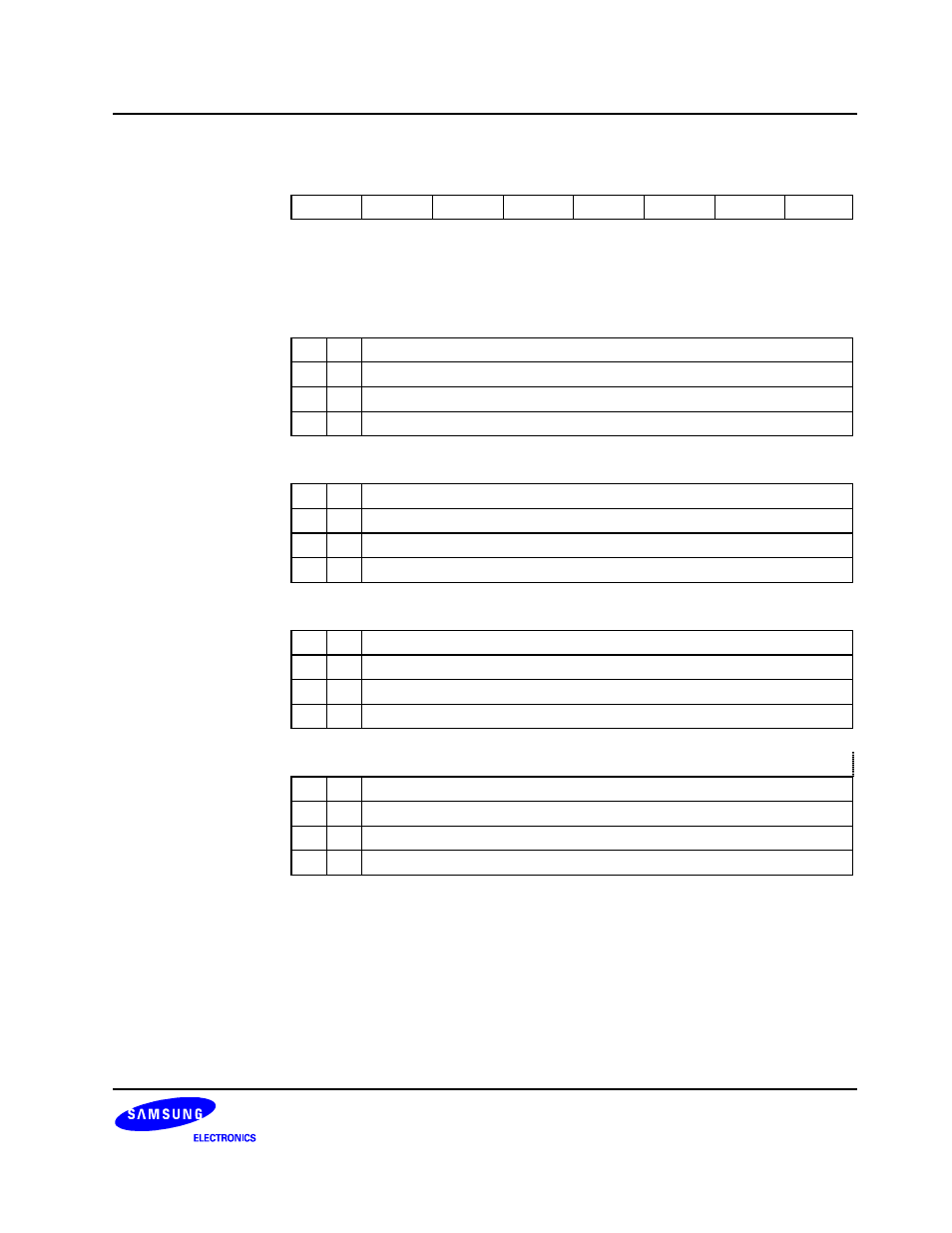
P2CONL
—
Port 2 Control Register (Low Byte)
EDH Set1 Bank0
Bit
Identifier
.7 .6 .5 .4 .3 .2 .1 .0
Reset Value
0 0 0 0 0 0 0 0
Read/Write
R/W R/W R/W R/W R/W R/W R/W R/W
Addressing Mode
Register addressing mode only
.7 and .6
P2.3/INT8 Mode Selection Bits
0
0
C-MOS input mode; interrupt on falling edges
0
1
C-MOS input mode; interrupt on rising edges and falling edges
1
0
Push-pull output mode
1
1
C-MOS input mode; interrupt on rising edges
.5 and .4
P2.2/INT7 Mode Selection Bits
0
0
C-MOS input mode; interrupt on falling edges
0
1
C-MOS input mode; interrupt on rising edges and falling edges
1
0
Push-pull output mode
1
1
C-MOS input mode; interrupt on rising edges
.3 and .2
P2.1/INT6 Mode Selection Bits
0
0
C-MOS input mode; interrupt on falling edges
0
1
C-MOS input mode; interrupt on rising edges and falling edges
1
0
Push-pull output mode
1
1
C-MOS input mode; interrupt on rising edges
.1 and .0
P2.0/INT5 Mode Selection Bits
0
0
C-MOS input mode; interrupt on falling edges
0
1
C-MOS input mode; interrupt on rising edges and falling edges
1
0
Push-pull output mode
1
1
C-MOS input mode; interrupt on rising edges
NOTE: Pull-up resistors can be assigned to individual port 2 pins by making the appropriate settings to the P2PUR control
register, location EEH, set 1,bank0.