Samsung S3F80JB User Manual
Page 248

S3F80JB
BASIC TIMER and TIMER 0
10-5
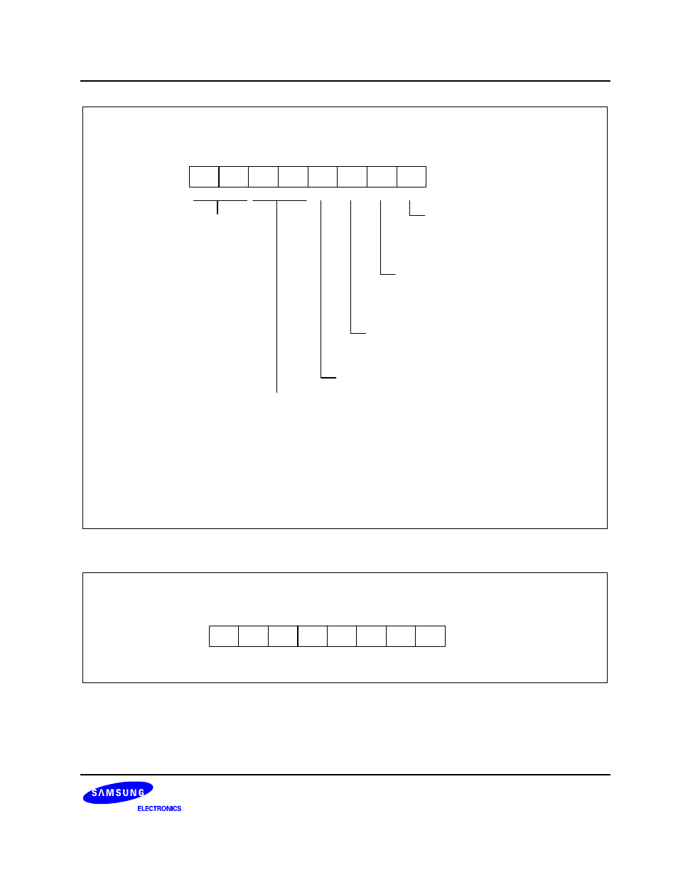
Timer 0 Control Register (T0CON)
D2H, Set 1, Bank0 , R/W
.7
.6
.5
.4
.3
.2
.1
.0
MSB
LSB
Timer 0 Interrupt Pending Bit:
0 = No interrupt pending
0 = Clear pending bit (when write)
1 = Interrupt is pending
Timer 0 Interrupt Match/capture Enable Bit:
0 = Disable interrupt
1 = Enable interrupt
Timer 0 Overflow Interrupt Enable Bit:
0 = Disable overflow interrupt
1 = Enable overflow interrupt
Timer 0 Input Clock Selection Bits:
00 = f
OSC
/4096
01 = f
OSC
/256
10 = f
OSC
/8
11 = External clock
(NOTE)
Timer 0 Counter Clear Bit:
0 = No effect
1 = Clear the timer 0 counter (when write)
Timer 0 Operating Mode Selection Bits:
00 = Interval mode
01 = Capture mode (capture on rising edge, counter running, OVF can occur)
10 = Capture mode (capture on falling edge, counter running, OVF can occur)
11 = PWM mode (OVF interrupt can occur)
NOTE:
The external clock source of timer 0 is P3.1/T0CK in 32-pin package, or P3.2/T0CK in 44-pin package.
Figure 10-2. Timer 0 Control Register (T0CON)
Timer 0 Data Register (T0DATA)
D1H, Set1, Bank 0 , R/W
.7
.6
.5
.4
.3
.2
.1
.0
MSB
LSB
Reset Value: FFH
Figure 10-3. Timer 0 DATA Register (T0DATA)
