Samsung S3F80JB User Manual
Page 242

I/O PORTS
S3F80JB
9-4
PORT DATA REGISTERS
Table 9-4 gives you an overview of the register locations of all four S3F80JB I/O port data registers. Data
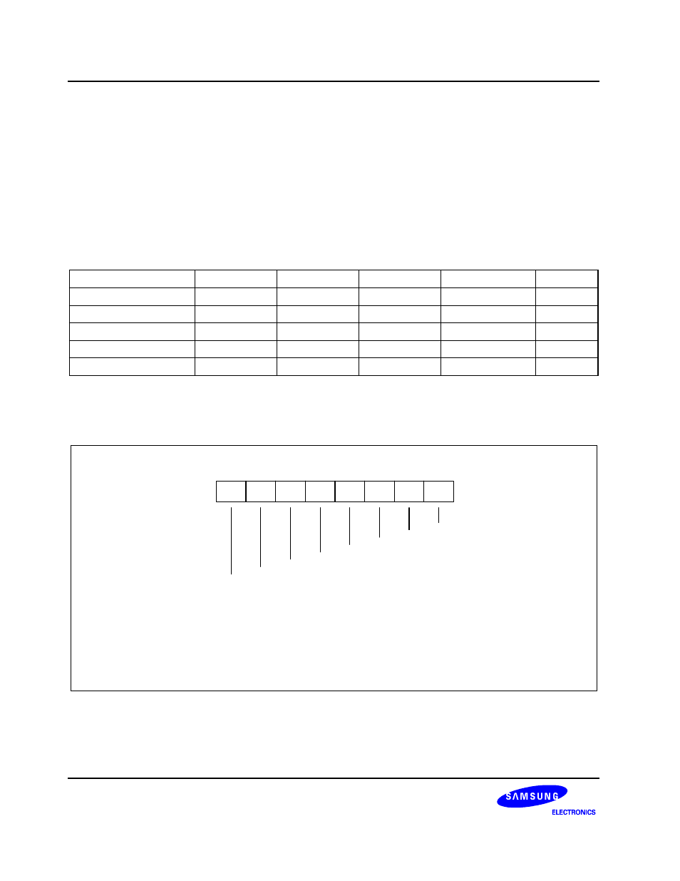
registers for ports 0,1,2 and 4 have the general format shown in Figure 9-1.
NOTE
The data register for port 3, P3, contains 6-bits for P3.0–P3.5, and an additional status bit (P3.7) for
carrier signal on/off.
Table 9-4. Port Data Register Summary
Register Name
Mnemonic
Decimal Hex Location
R/W
Port 0 data register
P0
224
E0H
Set 1, Bank 0
R/W
Port 1 data register
P1
225
E1H
Set 1, Bank 0
R/W
Port 2 data register
P2
226
E2H
Set 1, Bank 0
R/W
Port 3 data register
P3
227
E3H
Set 1, Bank 0
R/W
Port 4 data register
P4
228
E4H
Set 1, Bank 0
R/W
Because port 3 is a 6–bit I/O port, the port 3 data register only contains values for P3.0 – P3.5. The P3 register
also contains a special carrier on/off bit (P3.7). See the port3 description for details. All other I/O ports are 8–bit.
Pn.4
Pn.3
.7
.6
.5
.4
.3
.2
.1
.0
MSB
LSB
Pn.1
Pn.2
Pn.5
Pn.6
Pn.7
Pn.0
NOTE:
Because port 3 is a 6-bit I/O port, the port 3 data register only
contains values for P3.0-P3.5.
The P3 register also contains a special carrier on/off bit (P3.7).
See the port 3 description for details.
All other S3F80JB I/O ports are 8-bit.
Figure 9-1. S3F80JB I/O Port Data Register Format
