Cmod – Samsung S3F80JB User Manual
Page 75
CONTROL REGISTERS
S3F80JB
4-8
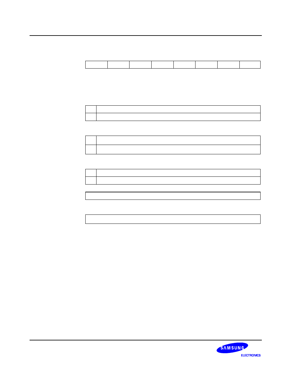
CMOD
—
Comparator Mode Register
E9H Set1 Bank1
Bit
Identifier
.7 .6 .5 .4 .3 .2 .1 .0
Reset Value
0 0 0 0 0 0 0 0
Read/Write
R/W R/W R/W R/W R/W R/W R/W R/W
Addressing Mode
Register addressing mode only
.7
Comparator Enable Bit
0
Comparator operation disable
1
Comparator operation enable
.6
Conversion Timer Control Bit
0
8
× 2
7
/ f
OSC
, 256 at 8 MHz
1
8
× 2
4
/ f
OSC
, 32 at 8 MHz
.5 External
Reference Selection Bit
0
Internal reference, CIN0-3: Analog input
1
External reference, CIN0-2: Analog input, CIN3: Reference input
.4
Not used for S3F80JB.
.3 – .0
Reference Voltage Selection Bits
Selected V
REF
= V
DD
× (N + 0.5)/16, N = 0 to 15
NOTE: You can select the number of analog input pin for your purpose by setting the CMPSEL.