T0con – Samsung S3F80JB User Manual
Page 108
S3F80JB
CONTROL REGISTERS
4-41
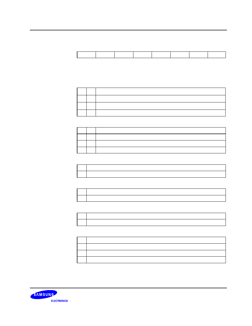
T0CON
— Timer 0 Control Register
D2H Set 1 Bank0
Bit
Identifier
.7 .6 .5 .4 .3 .2 .1 .0
Reset Value
0 0 0 0 0 0 0 0
Read/Write
R/W R/W R/W R/W R/W R/W R/W R/W
Addressing Mode
Register addressing mode only
.7 – .6
Timer 0 Input Clock Selection Bits
0 0
f
OSC
/4096
0 1
f
OSC
/256
1 0
f
OSC
/8
1
1
External clock input (at the T0CK pin, P3.1 or P3.2)
.5 and .4
Timer 0 Operating Mode Selection Bits
0
0
Interval timer mode (counter cleared by match signal)
0
1
Capture mode (rising edges, counter running, OVF interrupt can occur)
1
0
Capture mode (falling edges, counter running, OVF interrupt can occur)
1
1
PWM mode (Match and OVF interrupt can occur)
.3
Timer 0 Counter Clear Bit
0
No effect (when write)
1
Clear T0 counter, T0CNT (when write)
.2
Timer 0 Overflow Interrupt Enable Bit (note)
0
Disable T0 overflow interrupt
1 Enable
T0
overflow
interrupt
.1 Timer
0
Match/Capture Interrupt Enable Bit
0
Disable T0 match/capture interrupt
1
Enable T0 match/capture interrupt
.0 Timer
0
Match/Capture
Interrupt Pending Flag Bit
0
No T0 match/capture interrupt pending (when read)
0
Clear T0 match/capture interrupt pending condition (when write)
1
T0 match/capture interrupt is pending (when read)
1
No effect (when write)
NOTE: A timer 0 overflow interrupt pending condition is automatically cleared by hardware. However, the timer 0
match/capture interrupt, IRQ0, vector FCH, must be cleared by the interrupt service routine (S/W).