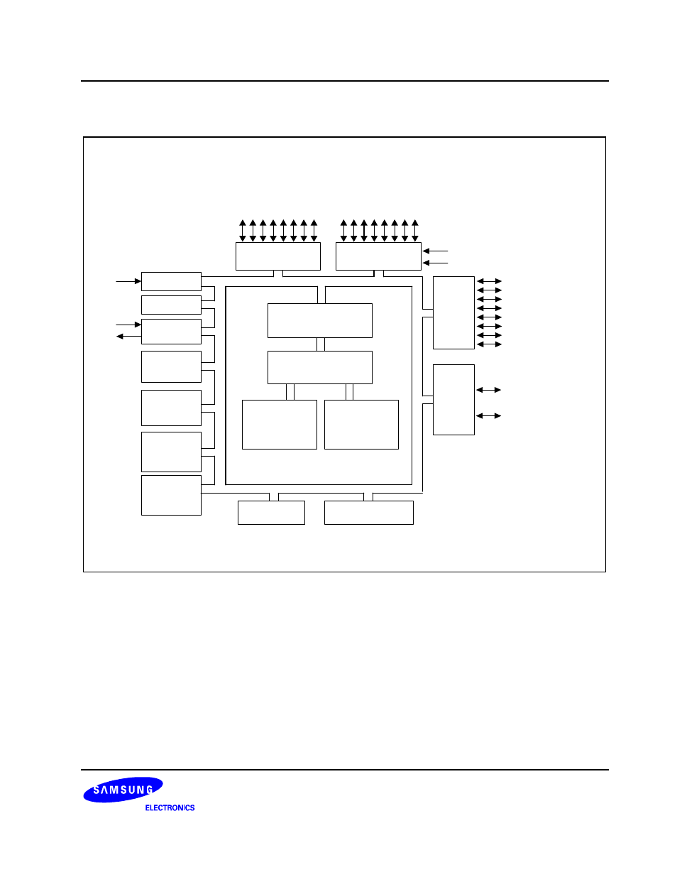
Block diagram (32-pin package) – Samsung S3F80JB User Manual
Page 21

S3F80JB
PRODUCT OVERVIEW
1-3
BLOCK DIAGRAM (32-PIN PACKAGE)
8-Bit
Timer0
/Counter
P0.0-0.3 (INT0-INT3)
P2.0-2.3
(INT5-INT8)
P2.4-2.7
(INT9)
(CIN0-CIN3)
P3.0/T0PWM/T0CAP/
SDAT/T1CAP/T2CAP
P3.1/REM/T0CK/SCLK
TEST
P0.4-P0.7(INT4)
P1.0-1.7
Port0
Port1
Port2
LVD
IPOR(note)
Main
OSC
8-Bit
Basic
Timer
16-Bit
Timer1
/Counter
16-Bit
Timer2
/Counter
I/O Port and Interrupt
Control
SAM8RC CPU
64K-byte
FLASH
Memory
272-byte
Register File
Port3
Comparator
Carrier Generator
(Counter A)
V
DD
X
IN
X
OUT
nRESET
Figure 1-1. Block Diagram (32-pin)
NOTE
IPOR can be enabled or disabled by IPOR / LVD control bit in the smart option. (Refer to Figure 2-2)
