Samsung S3F80JB User Manual
Page 276

COMPARATOR
S3F80JB
14-2
MUX
V
DD
Comparison
Result Register
(CMPREG)
MUX
MUX
MUX
CMPSEL_3
Ref (Internal)
SCAN
signal
Ref
(External)
R
R
+
-
1/2R
Internal BUS
NOTES:
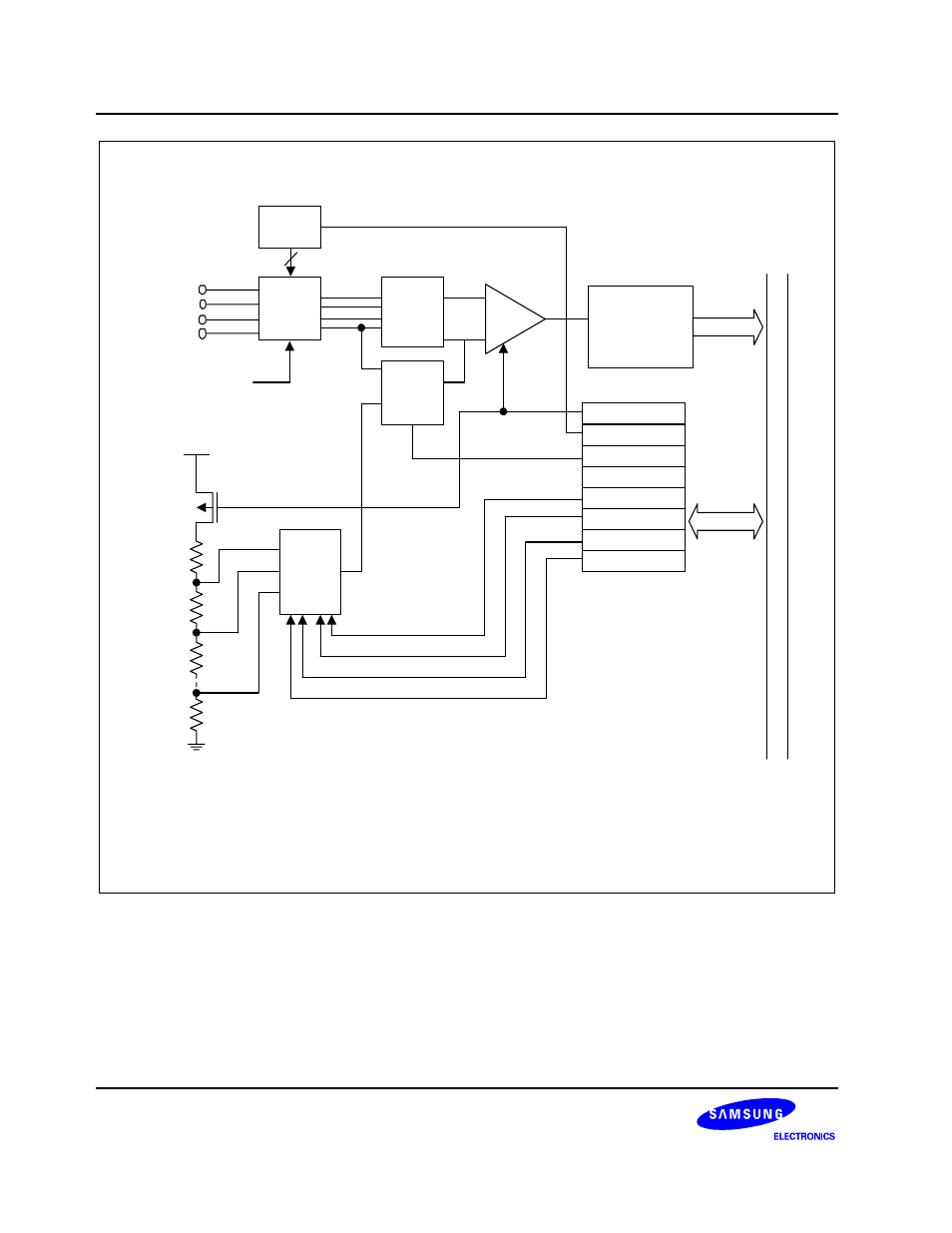
1. INT occurs only for digital input selecting. If an analog input, any INT doesn't occur.
2. The comparison results of CIN0,CIN1,CIN2 and CIN3 are respectively stored in
CMPREG0,CMPREG1,CMPREG2 and CMPREG3.
CMOD.7
CMOD.5
Not used
CMOD.3
CMOD.2
CMOD.1
CMOD.0
CMOD.6
CMPSEL_0
CMPSEL_1
CMPSEL_2
P2.4/CIN0
P2.5/CIN1
P2.6/CIN2
P2.7/CIN3
8
4
1/2R
Figure 14-1. Comparator Block Diagram for The S3F80JB
