Part 4 memory map, 1 introduction, 2 program map – Freescale Semiconductor 56F8122 User Manual
Page 30
56F8322 Techncial Data, Rev. 10.0
30
Freescale Semiconductor
Preliminary
Part 4 Memory Map
4.1 Introduction
The 56F8322 and 56F8122 devices are 16-bit motor-control chips based on the 56800E core. These parts
use a Harvard-style architecture with two independent memory spaces for Data and Program. On-chip
RAM and Flash memories are used in both spaces.
This section provides memory maps for:
•
Program Address Space, including the Interrupt Vector Table
•
Data Address Space, including the EOnCE Memory and Peripheral Memory Maps
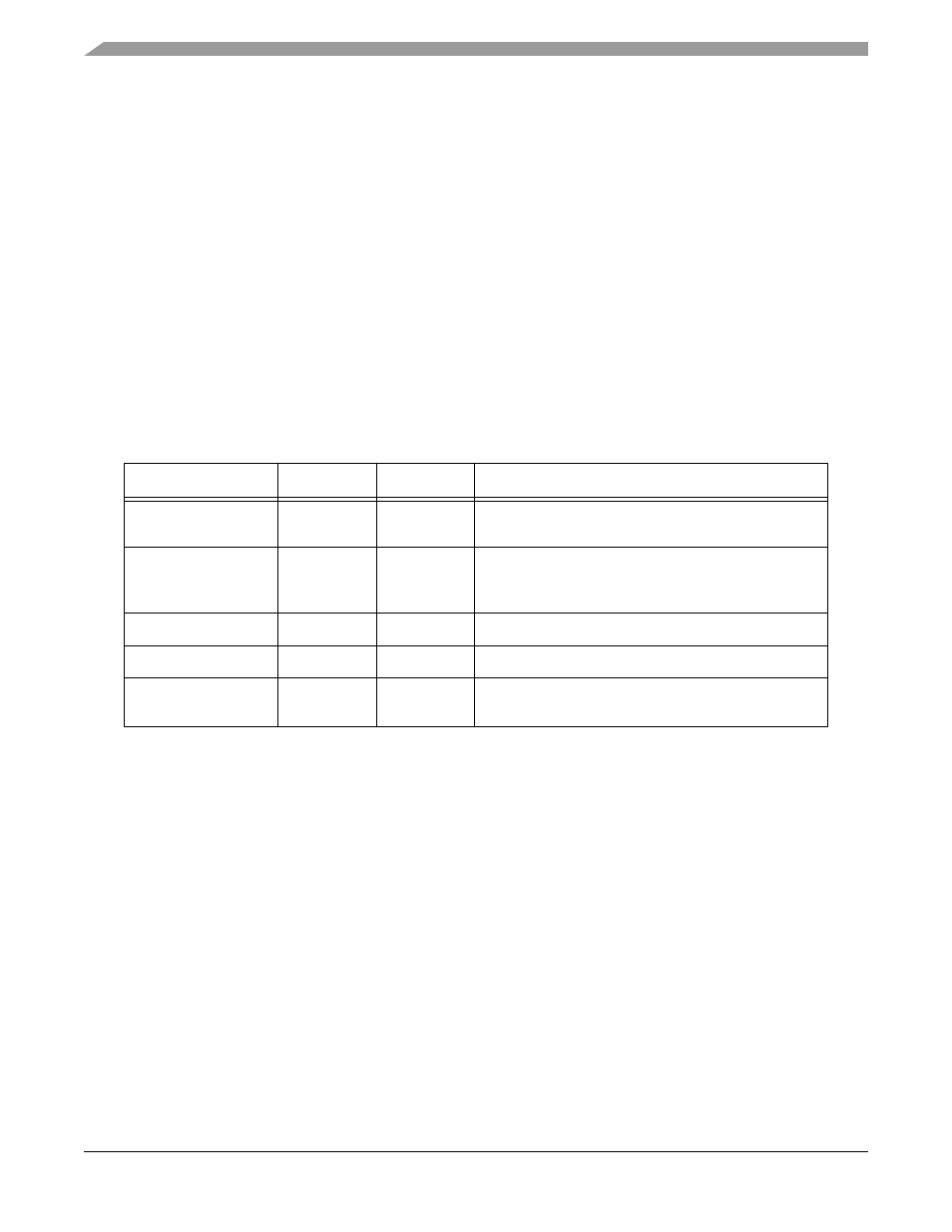
On-chip memory sizes for the device are summarized in
. Flash memories’ restrictions are
identified in the “Use Restrictions” column of
Note: Data Flash and Program RAM are NOT available on the 56F8122 device.
4.2 Program Map
The Program Memory map is located in
. The operating mode control bits (MA and MB) in the
Operating Mode Register (OMR) usually control the Program Memory map. Because the 56F8322 and
56F8122 do not include EMI, the OMR MA bit, which is used to decide internal or external BOOT, will
have no effect on the Program Memory Map. OMR MB reflects the security status of the Program Flash.
After reset, changing the OMR MB bit will have no effect on the Program Flash.
Table 4-1 Chip Memory Configurations
On-Chip Memory
56F8322
56F8122
Use Restrictions
Program Flash
32KB
32KB
Erase / Program via Flash interface unit and word writes
to CDBW
Data Flash
8KB
—
Erase / Program via Flash interface unit and word writes
to CDBW. Data Flash can be read via either CDBR or
XDB2, but not by both simultaneously.
Program RAM
4KB
—
None
Data RAM
8KB
8KB
None
Program Boot Flash
8KB
8KB
Erase / Program via Flash Interface unit and word
writes to CDBW