Freescale Semiconductor 56F8122 User Manual
Page 21
Signal Pins
56F8322 Technical Data, Rev. 10.0
Freescale Semiconductor
21
Preliminary
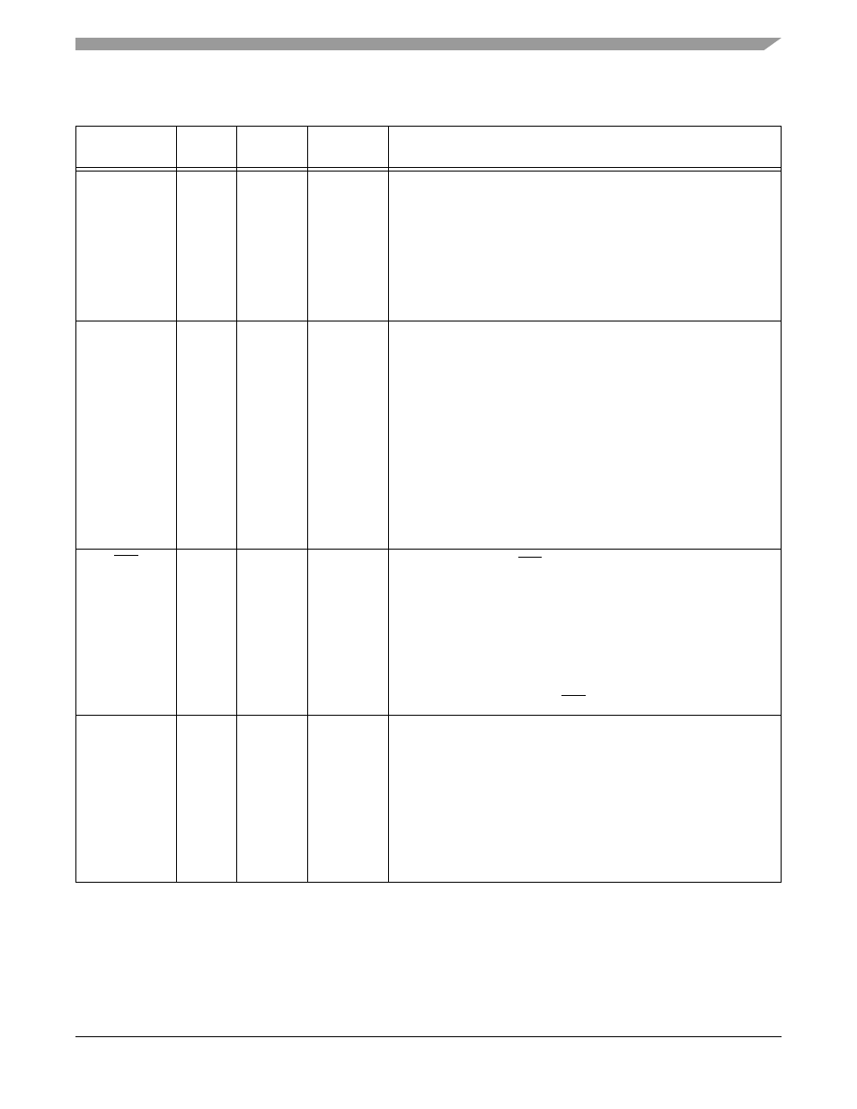
MOSI0
(GPIOB2)
18
Schmitt
Input/
Output
Schmitt
Input/
Output
Tri-stated
Input
SPI 0 Master Out/Slave In — This serial data pin is an output from a
master device and an input to a slave device. The master device
places data on the MOSI line a half-cycle before the clock edge the
slave device uses to latch the data.
Port B GPIO — This GPIO pin can be individually programmed as an
input or output pin.
After reset, the default state is MOSI0.
MISO0
(RXD1)
(GPIOB1)
16
Schmitt
Input/
Output
Schmitt
Input
Schmitt
Input/
Output
Input
Input
Input
SPI 0 Master In/Slave Out — This serial data pin is an input to a
master device and an output from a slave device. The MISO line of a
slave device is placed in the high-impedance state if the slave device
is not selected. The slave device places data on the MISO line a
half-cycle before the clock edge the master device uses to latch the
data.
Receive Data — SCI1 receive data input
Port B GPIO - This GPIO pin can be individually programmed as an
input or output pin.
After reset, the default state is MISO0.
SS0
(TXD1)
(GPIOB0)
15
Schmitt
Input
Schmitt
Output
Schmitt
Input/
Output
Input
Tri-stated
Input
SPI 0 Slave Select — SS0 is used in slave mode to indicate to the
SPI module that the current transfer is to be received.
Transmit Data — SCI1 transmit data output
Port B GPIO — This GPIO pin can be individually programmed as an
input or output pin.
After reset, the default state is SS0.
PWMA0
(GPIOA0)
3
Schmitt
Output
Schmitt
Input/
Output
Tri-stated
Input
PWMA0 — This is one of six PWMA output pins.
Port A GPIO — This GPIO pin can be individually programmed as an
input or output pin.
In the 56F8322, the default state after reset is PWMA0.
In the 56F8122, the default state is not one of the functions offered
and must be reconfigured.
Table 2-2 Signal and Package Information for the 48-Pin LQFP
Signal Name
Pin No.
Type
State During
Reset
Signal Description