Freescale Semiconductor 56F8122 User Manual
Page 40
56F8322 Techncial Data, Rev. 10.0
40
Freescale Semiconductor
Preliminary
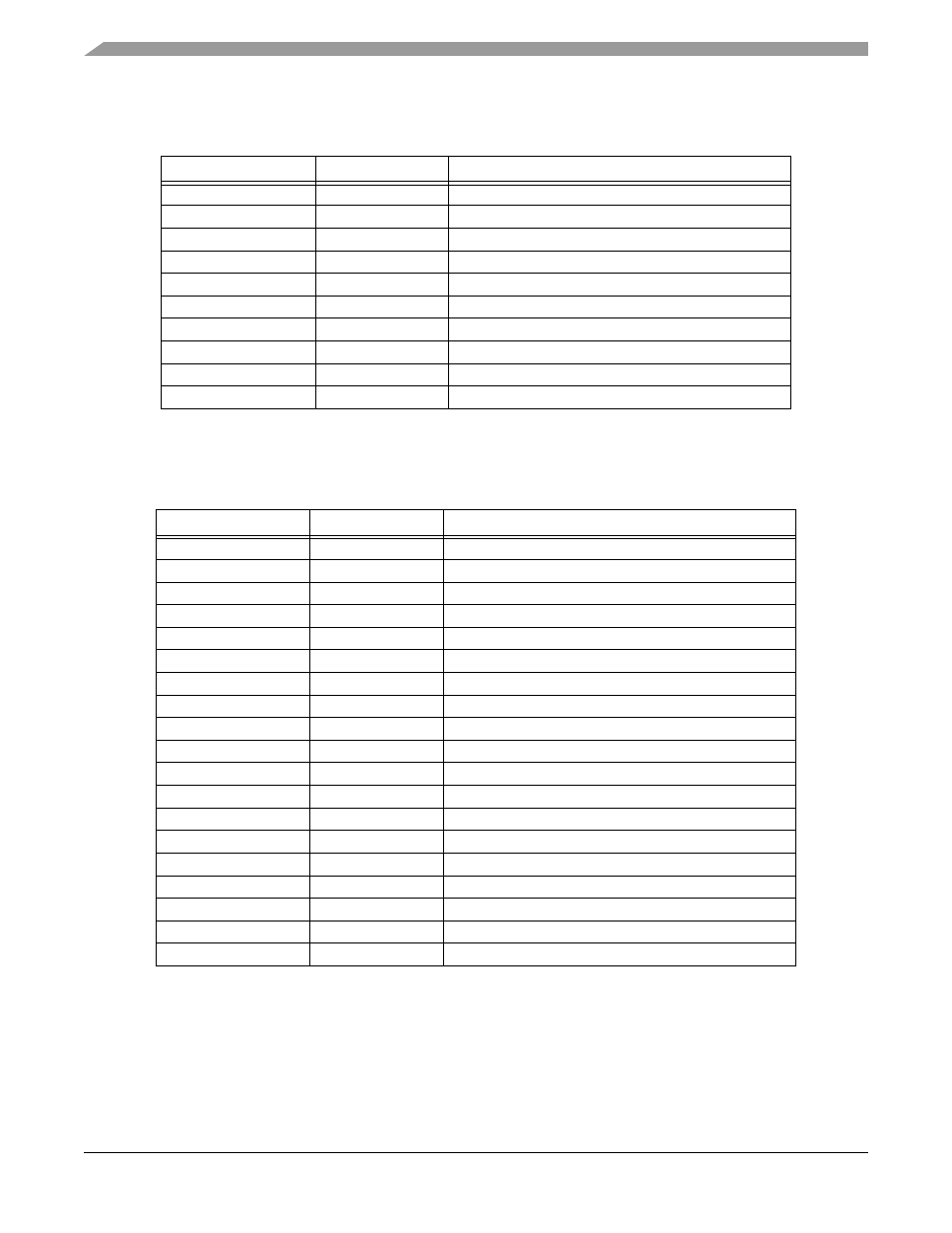
TMRC3_CMP2
$31
Compare Register 2
TMRC3_CAP
$32
Capture Register
TMRC3_LOAD
$33
Load Register
TMRC3_HOLD
$34
Hold Register
TMRC3_CNTR
$35
Counter Register
TMRC3_CTRL
$36
Control Register
TMRC3_SCR
$37
Status and Control Register
TMRC3_CMPLD1
$38
Comparator Load Register 1
TMRC3_CMPLD2
$39
Comparator Load Register 2
TMRC3_COMSCR
$3A
Comparator Status and Control Register
Table 4-10 Pulse Width Modulator A Registers Address Map
(PWMA_BASE = $00 F140)
PWM is NOT available in the 56F8122 device
Register Acronym
Address Offset
Register Description
PWMA_PMCTRL
$0
Control Register
PWMA_PMFCTRL
$1
Fault Control Register
PWMA_PMFSA
$2
Fault Status Acknowledge Register
PWMA_PMOUT
$3
Output Control Register
PWMA_PMCNT
$4
Counter Register
PWMA_PWMCM
$5
Counter Modulo Register
PWMA_PWMVAL0
$6
Value Register 0
PWMA_PWMVAL1
$7
Value Register 1
PWMA_PWMVAL2
$8
Value Register 2
PWMA_PWMVAL3
$9
Value Register 3
PWMA_PWMVAL4
$A
Value Register 4
PWMA_PWMVAL5
$B
Value Register 5
PWMA_PMDEADTM
$C
Dead Time Register
PWMA_PMDISMAP1
$D
Disable Mapping Register 1
PWMA_PMDISMAP2
$E
Disable Mapping Register 2
PWMA_PMCFG
$F
Configure Register
PWMA_PMCCR
$10
Channel Control Register
PWMA_PMPORT
$11
Port Register
PWMA_PMICCR
$12
Internal Correction Control
Table 4-9 Quad Timer C Registers Address Map (Continued)
(TMRC_BASE = $00 F0C0)
Register Acronym
Address Offset
Register Description