2 dc electrical characteristics, Table 10-5, Table 10-5 dc electrical characteristics – Freescale Semiconductor 56F8122 User Manual
Page 103
DC Electrical Characteristics
56F8322 Technical Data, Rev. 10.0
Freescale Semiconductor
103
Preliminary
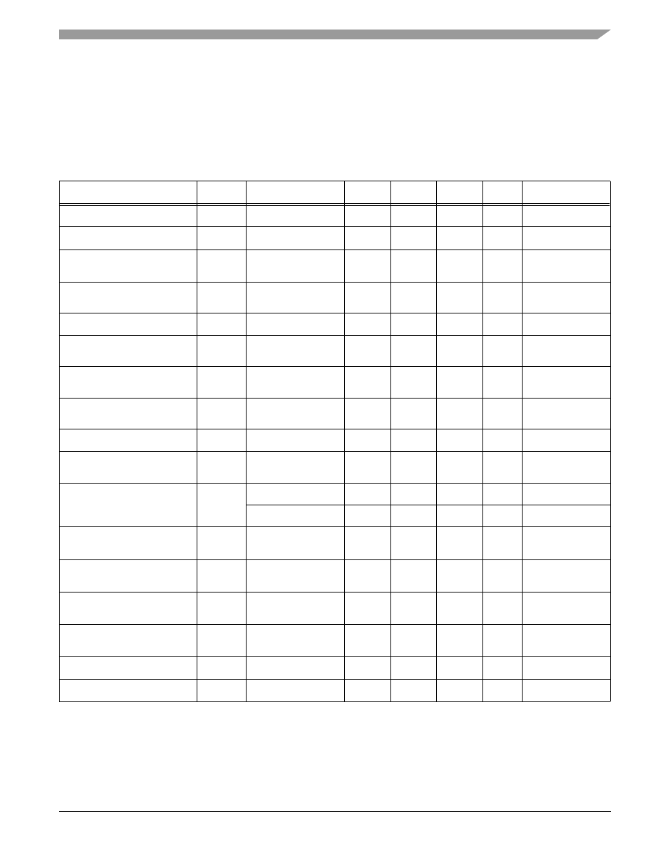
10.2 DC Electrical Characteristics
Note:
The 56F8122 device is specified to meet Industrial requirements only; PWM, CAN
and Quad Decoder are NOT available on the 56F8122 device.
See Pin Groups in
Table 10-5 DC Electrical Characteristics
At Recommended Operating Conditions; see
Characteristic
Symbol
Notes
Min
Typ
Max
Unit
Test Conditions
Output High Voltage
V
OH
2.4
—
—
V
I
OH
= I
OHmax
Output Low Voltage
V
OL
—
—
0.4
V
I
OL
= I
OLmax
Digital Input Current High
pull-up enabled or disabled
I
IH
Pin Groups
1, 3, 4
—
0
+/- 2.5
µ
A
V
IN
= 3.0V to 5.5V
Digital Input Current High
with pull-down
I
IH
Pin Group 5
40
80
160
µ
A
V
IN
= 3.0V to 5.5V
ADC Input Current High
I
IHADC
Pin Group 7
—
0
+/- 3.5
µ
A
V
IN
= V
DDA
Digital Input Current Low
pull-up enabled
I
IL
Pin Groups 1, 3, 4
-200
-100
-50
µ
A
V
IN
= 0V
Digital Input Current Low
pull-up disabled
I
IL
Pin Groups 1, 3, 4
—
0
+/- 2.5
µ
A
V
IN
= 0V
Digital Input Current Low
with pull-down
I
IL
Pin Group 5
—
0
+/- 2.5
µ
A
V
IN
= 0V
ADC Input Current Low
I
ILADC
Pin Group 7
—
0
+/- 3.5
µ
A
V
IN
= 0V
EXTAL Input Current Low
clock input
I
EXTAL
—
0
+/- 2.5
µ
A
V
IN
= V
DDA
or 0V
XTAL Input Current Low
clock input
I
XTAL
CLKMODE = High
—
0
+/- 2.5
µ
A
V
IN
= V
DDA
or 0V
CLKMODE = Low
—
—
200
µ
A
V
IN
= V
DDA
or 0V
Output Current
High Impedance State
I
OZ
Pin Groups 1, 2, 3
—
0
+/- 2.5
µ
A
V
OUT
= 3.0V to
5.5V or 0V
Schmitt Trigger Input
Hysteresis
V
HYS
Pin Groups 1, 3, 4, 5
—
0.3
—
V
—
Input Capacitance
(EXTAL/XTAL)
C
INC
—
4.5
—
pF
—
Output Capacitance
(EXTAL/XTAL)
C
OUTC
—
5.5
—
pF
—
Input Capacitance
C
IN
—
6
—
pF
—
Output Capacitance
C
OUT
—
6
—
pF
—