Table 10-1, Table 10-1 absolute maximum ratings – Freescale Semiconductor 56F8122 User Manual
Page 100
56F8322 Techncial Data, Rev. 10.0
100
Freescale Semiconductor
Preliminary
Note:
The 56F8122 device is specified to meet Industrial requirements only; PWM, CAN
and Quad Decoder are NOT available on the 56F8122 device.
Note: The overall life of this device may be reduced if subjected to extended use over 110°C junction. For additional information,
please contact your sales representative.
Note: Pins in italics are NOT available in the 56F8122 device.
Pin Group 1: TC0-1, FAULTA0, SS0, MISO0, MOSI0, SCLK0, HOME0, INDEX0, PHASEA0, PHASEB0, CAN_RX, CAN_TX
Pin Group 2: TDO
Pin Group 3: PWMA0-5
Pin Group 4: RESET, TMS, TDI, IRQA
Pin Group 5: TCK
Pin Group 6: XTAL, EXTAL
Pin Group 7: ANA0-6
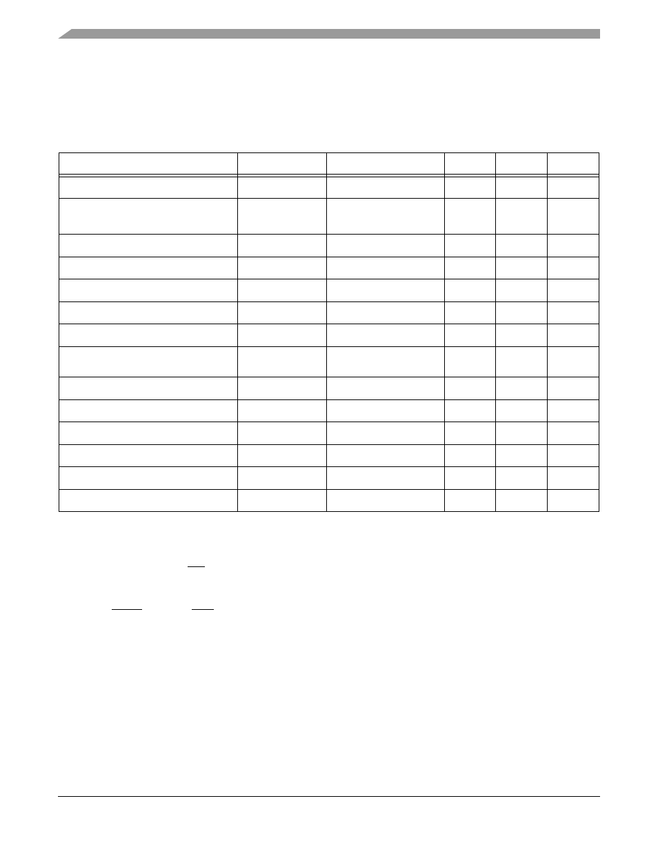
Table 10-1 Absolute Maximum Ratings
(V
SS
= V
SSA_ADC
= 0)
Characteristic
Symbol
Notes
Min
Max
Unit
Supply voltage
V
DD_IO
- 0.3
4.0
V
ADC Supply Voltage
V
DDA_ADC,
V
REFH
V
REFH
must be less than
or equal to
V
DDA_ADC
- 0.3
4.0
V
Oscillator / PLL Supply Voltage
V
DDA_OSC_PLL
- 0.3
4.0
V
Internal Logic Core Supply Voltage
V
DD_CORE
OCR_DIS is High
- 0.3
3.0
V
Input Voltage (digital)
V
IN
Pin Groups 1, 3, 4, 5
-0.3
6.0
V
Input Voltage (analog)
V
INA
Pin Group 7
-0.3
4.0
V
Output Voltage
V
OUT
Pin Groups 1, 2, 3
-0.3
4.0
V
Output Voltage (open drain)
V
OD
GPIO pins used in open
drain mode
-0.3
6.0
V
Ambient Temperature (Automotive)
T
A
-40
125
°C
Ambient Temperature (Industrial)
T
A
-40
105
°C
Junction Temperature (Automotive)
T
J
-40
150
°C
Junction Temperature (Industrial)
T
J
-40
125
°C
Storage Temperature (Automotive)
T
STG
-55
150
°C
Storage Temperature (Industrial)
T
STG
-55
150
°C