5 external clock operation timing, Table 10-13, Spi t – Freescale Semiconductor 56F8122 User Manual
Page 109
External Clock Operation Timing
56F8322 Technical Data, Rev. 10.0
Freescale Semiconductor
109
Preliminary
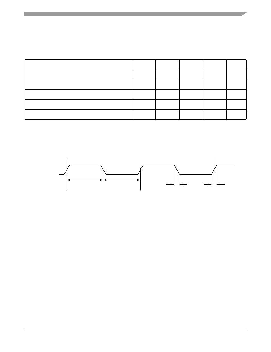
10.5 External Clock Operation Timing
Figure 10-3 External Clock Timing
Table 10-13 External Clock Operation Timing Requirements
1
1. Parameters listed are guaranteed by design.
Characteristic
Symbol
Min
Typ
Max
Unit
Frequency of operation (external clock driver)
2
—56F8322
2. See
for details on using the recommended connection of an external clock driver.
f
osc
0
—
120
MHz
Frequency of operation (external clock driver)
2
—56F8122
f
osc
0
—
80
MHz
Clock Pulse Width
3
3. The high or low pulse width must be no smaller than 8.0ns or the chip will not function.
t
PW
3.0
—
—
ns
External clock input rise time
4
4. External clock input rise time is measured from 10% to 90%.
t
rise
—
—
15
ns
External clock input fall time
5
5. External clock input fall time is measured from 90% to 10%.
t
fall
—
—
15
ns
External
Clock
V
IH
V
IL
Note: The midpoint is V
IL
+ (V
IH
– V
IL
)/2.
90%
50%
10%
90%
50%
10%
t
PW
t
PW
t
fall
t
rise