3 power distribution and i/o ring implementation, Section 12.3, Figure 12-1 – Freescale Semiconductor 56F8122 User Manual
Page 134
56F8322 Techncial Data, Rev. 10.0
134
Freescale Semiconductor
Preliminary
•
Because the device’s output signals have fast rise and fall times, PCB trace lengths should be minimal
•
Consider all device loads as well as parasitic capacitance due to PCB traces when calculating capacitance.
This is especially critical in systems with higher capacitive loads that could create higher transient currents
in the V
DD
and V
SS
circuits.
•
Take special care to minimize noise levels on the V
REF
, V
DDA
and V
SSA
pins
•
Because the Flash memory is programmed through the JTAG/EOnCE port, the designer should provide an
interface to this port to allow in-circuit Flash programming
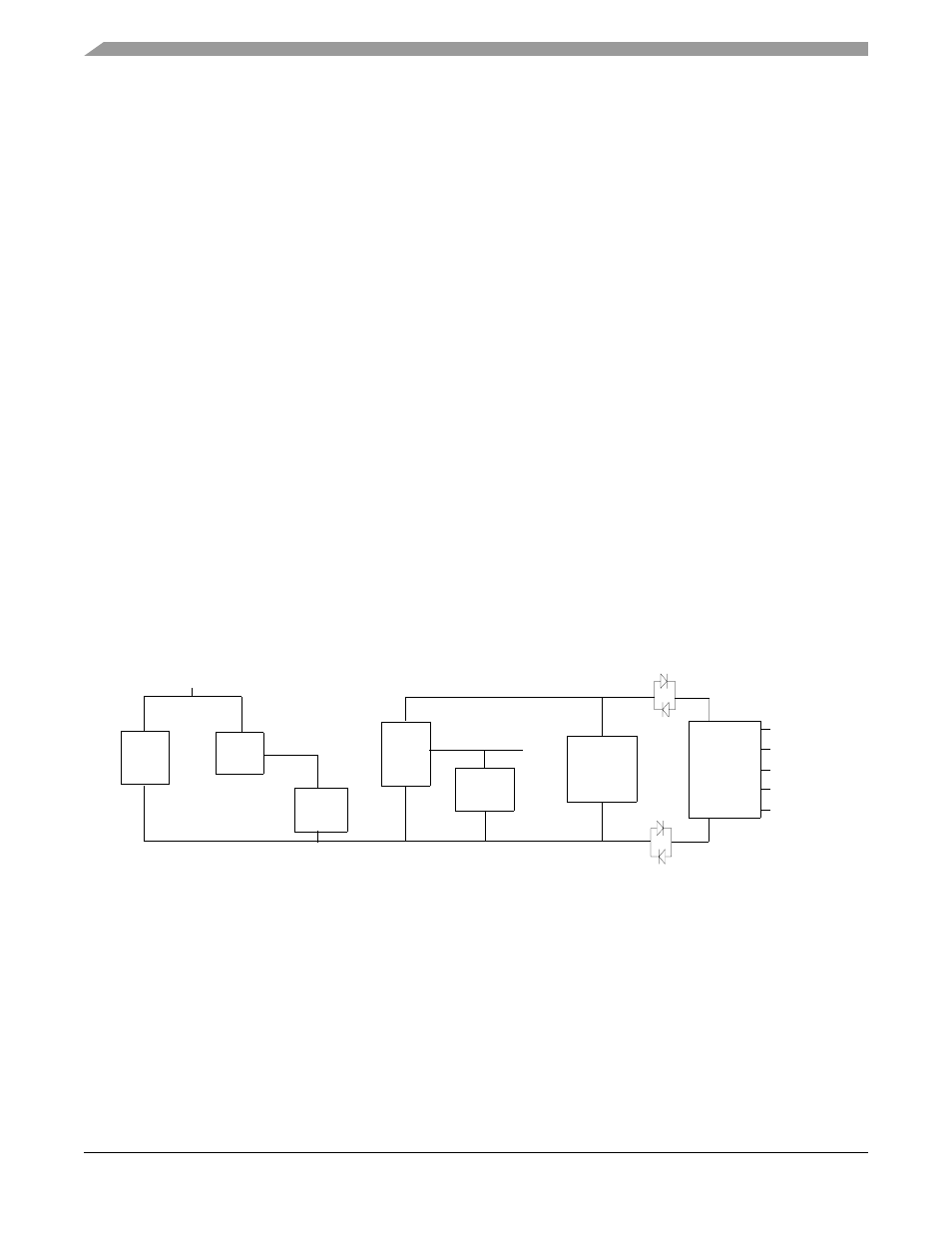
12.3 Power Distribution and I/O Ring Implementation
illustrates the general power control incorporated in the 56F8322/56F8122. This chip
contains two internal power regulators. One of them is powered from the V
DDA_OSC_PLL
pin and cannot
be turned off. This regulator controls power to the internal clock generation circuitry. The other regulator
is powered from the V
DD_IO
pins and provides power to all of the internal digital logic of the core, all
peripherals and the internal memories. This regulator can be turned off, if an external V
DD_CORE
voltage
is externally applied to the V
CAP
pins.
In summary, the entire chip can be supplied from a single 3.3 volt supply if the large core regulator is
enabled. If the regulator is not enabled, a dual supply 3.3V/2.5V configuration can also be used.
Notes:
•
Flash, RAM and internal logic are powered from the core regulator output
•
V
PP
1 and V
PP
2 are not connected in the customer system
•
All circuitry, analog and digital, shares a common V
SS
bus
Figure 12-1 Power Management
REG
CORE
V
CAP
I/O
ADC
V
DD
V
SS
OCS
REG
V
DDA_OSC_PLL
ROSC
V
SSA_ADC
V
DDA_ADC
V
REFH
V
REFP
V
REFMID
V
REFN
V
REFLO