Table 4-3 interrupt vector table contents, Continued) – Freescale Semiconductor 56F8122 User Manual
Page 33
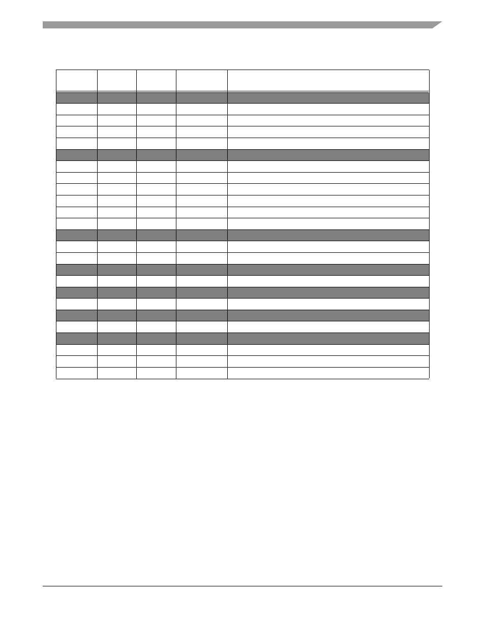
Interrupt Vector Table
56F8322 Technical Data, Rev. 10.0
Freescale Semiconductor
33
Preliminary
Reserved
TMRC
56
0-2
P:$70
Timer C Channel 0
TMRC
57
0-2
P:$72
Timer C Channel 1
TMRC
58
0-2
P:$74
Timer C Channel 2
TMRC
59
0-2
P:$76
Timer C Channel 3
Reserved
TMRA
64
0-2
P:$80
Timer A Channel 0
TMRA
65
0-2
P:$82
Timer A Channel 1
TMRA
66
0-2
P:$84
Timer A Channel 2
TMRA
67
0-2
P:$86
Timer A Channel 3
SCI0
68
0-2
P:$88
SCI 0 Transmitter Empty
SCI0
69
0-2
P:$8A
SCI 0 Transmitter Idle
Reserved
SCI0
71
0-2
P:$8E
SCI 0 Receiver Error
SCI0
72
0-2
P:$90
SCI 0 Receiver Full
Reserved
ADCA
74
0-2
P:$94
ADC A Conversion Complete / End of Scan
Reserved
ADCA
76
0-2
P:$98
ADC A Zero Crossing or Limit Error
Reserved
PWMA
78
0-2
P:$9C
Reload PWM A
Reserved
PWMA
80
0-2
P:$A0
PWM A Fault
core
81
- 1
P:$A2
SW Interrupt LP
82
0 - 2
P:$A4
1. Two words are allocated for each entry in the vector table. This does not allow the full address range to be referenced
from the vector table, providing only 19 bits of address.
2. If the VBA is set to $0200, the first two locations of the vector table will overlay the chip reset addresses.
Table 4-3 Interrupt Vector Table Contents
1
(Continued)
Peripheral
Vector
Number
Priority
Level
Vector Base
Address +
Interrupt Function