13 controller area network (can) timing, 14 jtag timing, Table 10-23 – Freescale Semiconductor 56F8122 User Manual
Page 120: Table 10-22 can timing, Table 10-23 jtag timing
56F8322 Techncial Data, Rev. 10.0
120
Freescale Semiconductor
Preliminary
10.13 Controller Area Network (CAN) Timing
Note: CAN is NOT available in the 56F8122 device.
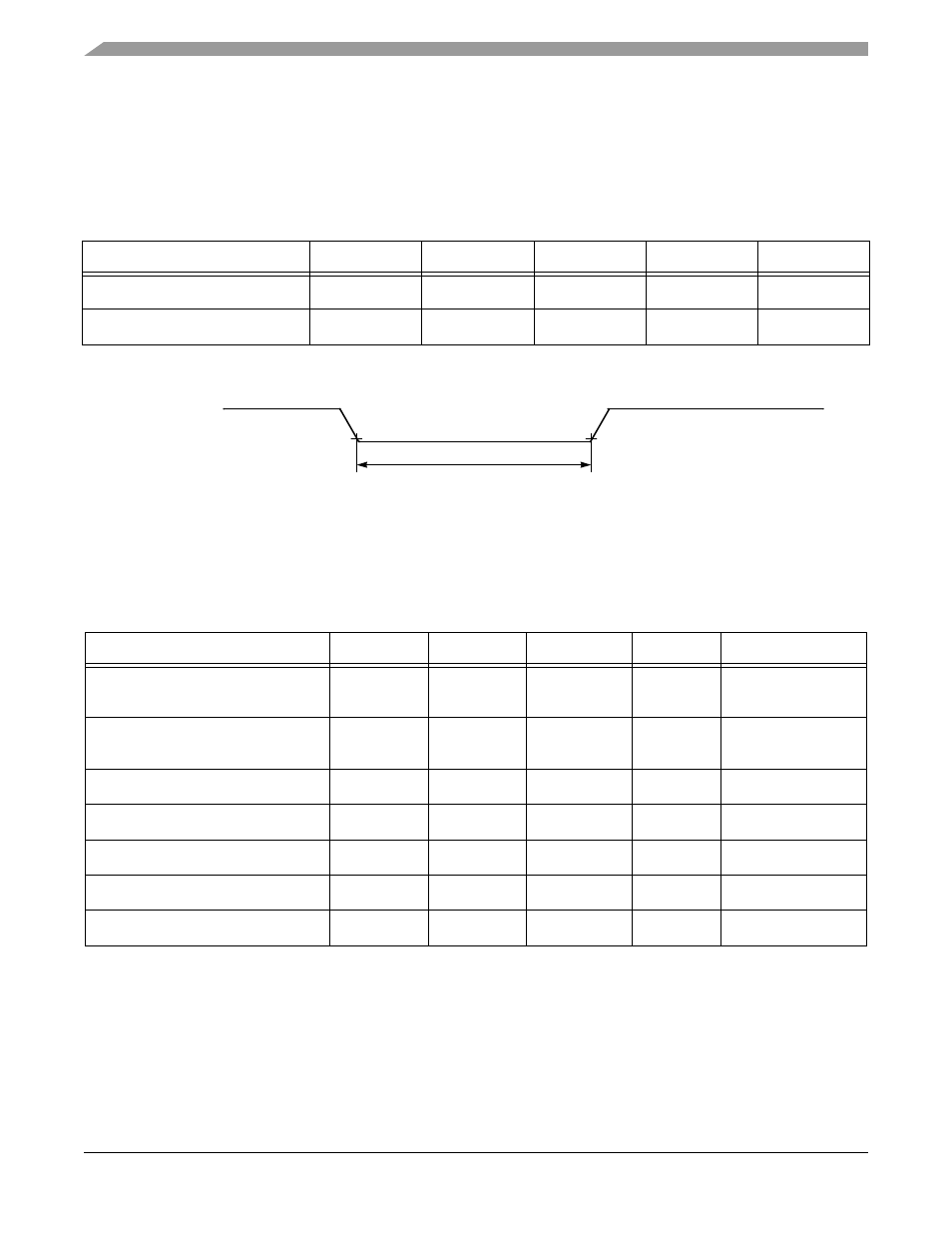
Figure 10-17 Bus Wakeup Detection
10.14 JTAG Timing
Table 10-22 CAN Timing
1
1. Parameters listed are guaranteed by design
Characteristic
Symbol
Min
Max
Unit
See Figure
Baud Rate
BR
CAN
—
1
Mbps
—
Bus Wake-up detection
T
WAKEUP
T
IPBUS
—
µ
s
Table 10-23 JTAG Timing
Characteristic
Symbol
Min
Max
Unit
See Figure
TCK frequency of operation using
EOnCE
1
1. TCK frequency of operation must be less than 1/8 the processor rate.
f
OP
DC
SYS_CLK/8
MHz
TCK frequency of operation not
using EOnCE
1
f
OP
DC
SYS_CLK/4
MHz
TCK clock pulse width
t
PW
50
—
ns
TMS, TDI data set-up time
t
DS
5
—
ns
TMS, TDI data hold time
t
DH
5
—
ns
TCK low to TDO data valid
t
DV
—
30
ns
TCK low to TDO tri-state
t
TS
—
30
ns
T
WAKEUP
MSCAN_RX
CAN receive
data pin
(Input)