12 serial communication interface (sci) timing, Figure 10-14 quadrature decoder timing – Freescale Semiconductor 56F8122 User Manual
Page 119
Serial Communication Interface (SCI) Timing
56F8322 Technical Data, Rev. 10.0
Freescale Semiconductor
119
Preliminary
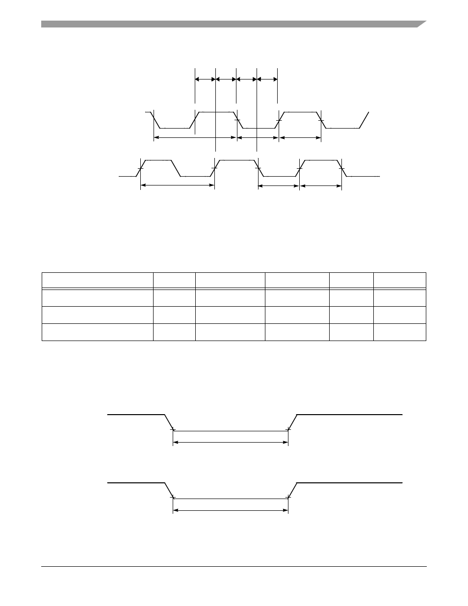
Figure 10-14 Quadrature Decoder Timing
10.12 Serial Communication Interface (SCI) Timing
Figure 10-15 RXD Pulse Width
Figure 10-16 TXD Pulse Width
Table 10-21 SCI Timing
1
1. Parameters listed are guaranteed by design.
Characteristic
Symbol
Min
Max
Unit
See Figure
Baud Rate
2
2. f
MAX
is the frequency of operation of the system clock in MHz, which is 60MHz for the 56F8322 device and 40MHz for the
56F8122 device.
BR
—
(f
MAX
/16)
Mbps
—
RXD
3
Pulse Width
3. The RXD pin in SCI0 is named RXD0 and the RXD pin in SCI1 is named RXD1.
RXD
PW
0.965/BR
1.04/BR
ns
TXD
4
Pulse Width
4. The TXD pin in SCI0 is named TXD0 and the TXD pin in SCI1 is named TXD1.
TXD
PW
0.965/BR
1.04/BR
ns
Phase B
(Input)
P
IN
P
HL
P
HL
Phase A
(Input)
P
IN
P
HL
P
HL
P
PH
P
PH
P
PH
P
PH
RXD
PW
RXD
SCI receive
data pin
(Input)
TXD
PW
TXD
SCI receive
data pin
(Input)