I it – Epson 4003353 User Manual
Page 44
stylus
The
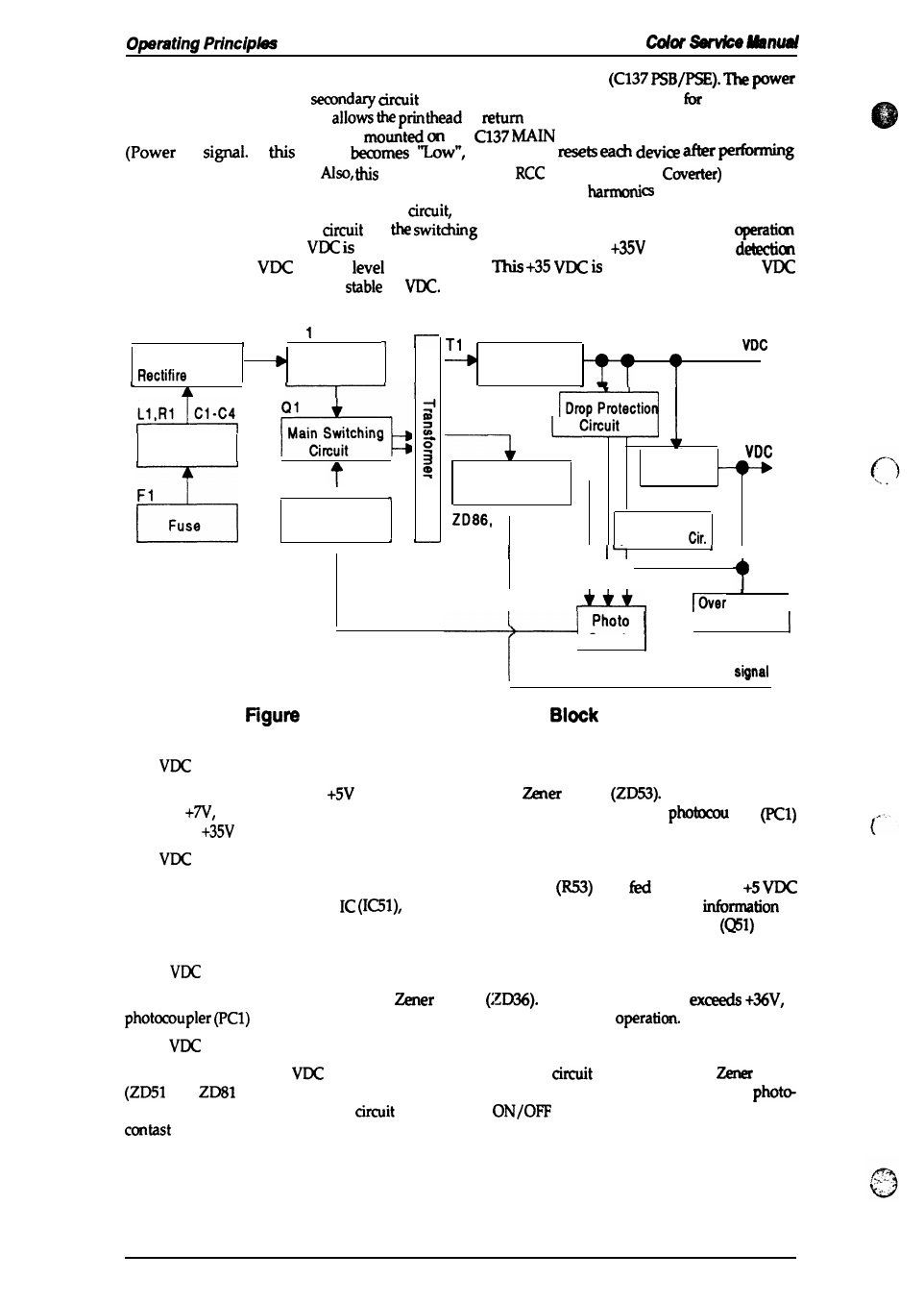
figure below shows a block diagram of the power supply circuit
switch is equipped with a
that allows the CPU to remain active
a while after
the printer is
turned off. This
to
to the capping position after power has
been turned off. The CPU that is
the
board always monitors the PSC
@/
~
If
signal
the
CPU
the
head capping sequence.
board employs the
(Ringing Choke
switching
system. This AC voltage is first input to the filter circuit for higher
absorption, and then
input to the rectification and smoothing
converting it into DC voltage. This DC voltage is
then input to the switching
for
operation. Along with the switching
on the primary
side, +35
generated after passing through the
line voltage
circuit. This
+35
output
is stabilized.
also input to the +5
generation circuit to generate a
+5
DB1
cl
Full-wave
Smoothing
Circuit
Circuit
I
Filter Circuit
Fuse
I
Feed back
Circuit
4
C51
Smoothing
+35
➤
Circuit
ZD51 , 81-84
‘
+5
P-off Detection
TL 494
and delay circuit
A
ZD52
Over voltage
C82
protection
I
I
I It
ZD53
I
voltage I
[protection Cir.
I
Coupler
P c l
P-OFF
2-17. Power Supply Circuit
Diagram
1)+5
line overvoltage protection circuit
The output voltage level of
line is monitored by a
diode
If the voltage
level
exceeds
the status
is fed back to the primary switching circuit through a
pier
to stop the
generation.
2)+5
line over current/ overvoltage control circuit.
The output current is monitored by a detection resistor
and
back to the
generation switching control
which monitors the output voltage. This
is
input to the internal comparator and outputs the high signal to turn off the transistor
when
the voltage or the current becomes abnormal.
3) +35
line overvoltage protection circuit
The output level is monitored by a
diode
If the voltage level
a
is activated; stopping the primary switching circuit
4) +35
line drop protection circuit
The output level of +35
line is monitored by a detection
that consists of a
diode
and
to 84). This circuit feeds back the output voltage level status through a
coupler to the primary switching
to control the
time of the switching transistor for
output voltage.
2-14
Rev.
A