ProSoft Technology PLX31-EIP-SIE User Manual
Page 180

SIE Protocol
PLX3x Series
User Manual
Ethernet and Serial Gateways
Page 180 of 218
ProSoft Technology, Inc.
September 17, 2014
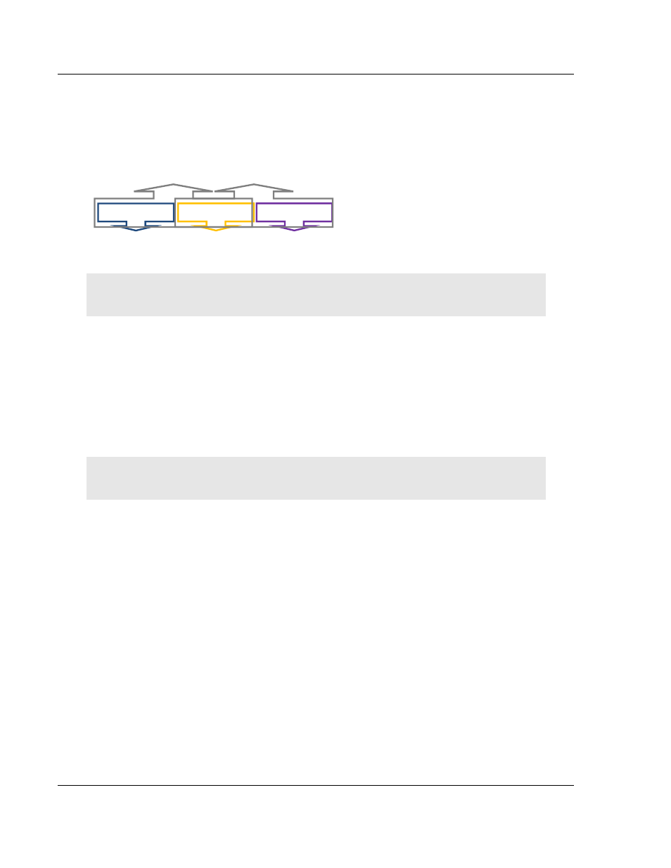
The second byte of DB1.DBW0 is the same as DB1.DBB1, and is the same as
the first byte of DB1.DBW1.
In reality, the memory space looks like below:
DB1.DBW0 DB1.DBW1
2#0010_1101 2#1101_0101 2#0101_0111
DB1.DBB0 DB1.DBB1 DB1.DBB2
Note: To access the first address of Data Block, Flag, Input, Output, Timer, and Counter memory
locations in the S7-300 and S7-1200 processors, use the following address syntax.
Data Block -> DB1.DBB0, DB1.DBW0, DB1.DBD0
Flag -> MB0, MW0, MD0
Input -> IB0, IW0, ID0
Output -> QB0, QW0, QD0
Timers -> T0
– T65535
Counters -> C0
– C65535
Note: To access the first address of Data Block, Flag, Input and Output memory locations in the
S7-200 processor, use the following address syntax.
Data Block -> VB0, VW0, VD0
Flag -> MB0, MW0, MD0
Input -> IB0, IW0, ID0
Output -> QB0, QW0, QD0
