3 functional description, 1 block diagram, 2 module description – Sundance SMT943 User Manual
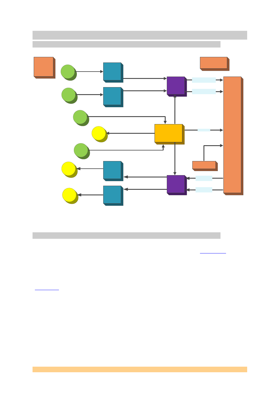
Page 8: Figure 1 - smt943 block diagram
User Manual SMT943
Last Edited: 23/08/2011 17:24:00
3 Functional Description
3.1 Block Diagram
S
L
B
I
n
te
rf
a
c
e
c
o
n
n
e
c
to
r
ADS62P49
Dual ADC Ch A
& Ch B
14-bit
250MSPS
(2x 675mW)
DAC5688
Dual channel
DAC
16-Bit
800MSPS
Interpolation
(1.3W)
Clock Synchronizer and
Jitter cleaner
Based on
CDCE72010
(1.8W)
Channel B
Signal
Conditioning
(AC coupling)
Channel A
Signal
Conditioning
(AC coupling)
Channel B
Signal
Conditioning
(AC coupling)
Channel A
Signal
Conditioning
(AC coupling)
DAC
Output
Ch A
MMCX
50 Ohm
DAC
Output
Ch B
MMCX
50 Ohm
ADC Input
Ch A
MMCX
50 Ohm
ADC Input
Ch B
MMCX
50 Ohm
ADCs
External
Clock in
MMCX
External
Refference
Clock in
MMCX
ADCs
External
Clock out
MMCX
Ch A
– 1.8V DDR LVDS
Clock and Control
Ch B
– 1.8V DDR LVDS
Clock and Control
Ch A
– Data (16)
and Control
Ch B
– Data (16)
and control
SLB Power connector
External Trigger
FPGA Clock
SMT943
ADC / DAC
Module, 2 ADC
Channels; 250MHz
@ 14 bits; 2 DACs
@ 800MHz/16 bits
Power Supplies:
1.8 and 3.3V
Linear
Regulators
Figure 1 - SMT943 Block diagram.
3.2 Module Description
The SMT943 has got 1 dual channel Analog-to-Digital converters
– Texas
Instrument) that has been designed for multi-carrier, wide bandwidth
communication applications. Both analog inputs are available on MMCX connectors.
They are 50-Ohm AC-coupled inputs (RF transformers - ration 1). DDR LVDS lines
are used to carry samples through the SLB connector to the FPGA (SLB base module -
FPGA IOs must be set to 2.5-Volt). The module has also got a dual channel DAC
– Texas Instrument) that has integrated 2x-8x interpolation filters, a fine
frequency mixer with a 32-bit complex numerically controlled oscillator, an on-
board clock multiplier, an IQ compensation and an internal voltage reference.
A clock distribution chip ensures that all converters sample synchronously to a
single clock source. The clock source can be external or internal (on-board 491.52-
MHz VCXO). The distribution chip also allows synchronising the on-board VCXO to a
reference signal that can be external or internal (on-board 10-MHz crystal). External
reference, external sampling clock input and output are accessible on MMCX
connectors. An external trigger input is also available on the board.
All control, data and clock lines are mapped onto an SLB connector so the card can
be fully controlled by an SLB FPGA base module (SMT351T for example).