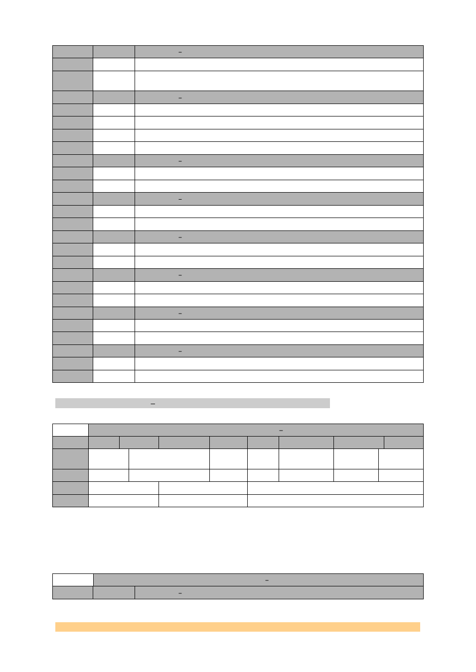
Dac chcd register 1 0x41 – Sundance SMT943 User Manual
Page 42
User Manual SMT943
Page 42 of 54
Last Edited: 23/08/2011 17:24:00
Setting
Bit 2
Description synchr_clkin
0
0
Synchronous mode off.
1
1
Synchronous mode on. Clk1 and Clk2 must synchronous in phase and frequency when
reaching the DAC
Setting
Bit 7:6
Description insel mode
0
00
Normal input on Port A and Port B.
1
01
Interleaved input on Port A.
2
10
Interleaved input on Port B.
3
11
Half rate on Port A and B.
Setting
Bit 8
Description mixer_ena
0
0
Mixer bypassed.
1
1
Mixer enabled.
Setting
Bit 9
Description qmc_corr_ena
0
0
QMC phase and gain correction bypasses.
1
1
QNC phase and gain correction enabled.
Setting
Bit 10
Description qmc_offset_ena
0
0
QMC offset correction bypasses.
1
1
QNC offset correction enabled.
Setting
Bit 11
Description fir4_ena
0
0
Filter bypassed.
1
1
FIR4 Inverse Sinc filter enabled.
Setting
Bit 13
Description clk1c_in_ena
0
0
Pin used as PLL_LOCK status output.
1
1
Pin used as a clock input.
Setting
Bit 14
Description clk1_in_ena
0
0
Pin used as CLK0 clock output.
1
1
Pin used as a clock input.
DAC chcd Register 1 0x41.
DAC chcd Register 1 0x41
Byte
Bit 7
Bit 6
Bit 5
Bit 4
Bit 3
Bit 2
Bit 1
Bit 0
1
Ser_dac_d
ata_ena
Output delay
b_equals
_a
A_equa
ls_b
reserved
revb
reva
Default
‘0’
‘00’
‘0’
‘0’
‘0’
‘0’
‘0’
0
Diffclk_dly
Clk0_dly
Reserved
Default
‘00’
‘00’
‘0000’
DAC chcd Register 1 0x41
Setting
Bit 5:4
Description clk0_dly