Clock register 1 0x11, Clock register 2 0x12 – Sundance SMT943 User Manual
Page 22
User Manual SMT943
Page 22 of 54
Last Edited: 23/08/2011 17:24:00
1
01
2
10
3
11
Setting
Bit 12
Description CP_MODE
0
0
3V.
1
1
5V
Setting
Bit 13
Description CP_DIR
0
0
Positive CP current output
1
1
Negative CP current output
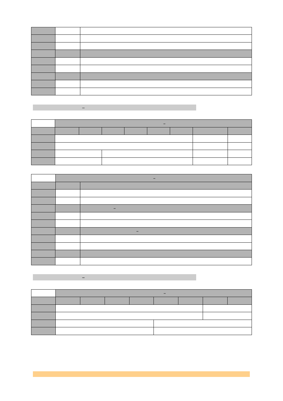
CLOCK Register 1 0x11.
Clock Register 1 0x11
Byte
Bit 7
Bit 6
Bit 5
Bit 4
Bit 3
Bit 2
Bit 1
Bit 0
1
Output0 (DAC chc&d clk1) Mode
PECLOHISWING
Reserved
Default
‘100000’
‘0’
‘0’
0
Reserved
ICP
CP_PRE
Reserved
Default
‘00’
‘0000’
‘0’
‘0’
Reset Register 1 0x11
Setting
Bit 1
Description CP_PRE - Preset charge pump output voltage to vcc/2
0
0
OFF.
1
1
ON.
Setting
Bit 5:2
Description ICP Charge pump current setting
0
0
1
1
Setting
Bit 9
Description PECL0HISWING PECL output voltage swing (DAC chc&d clk1)
0
0
Normal Operation.
1
1
High PECL output voltage.
Setting
Bit 15:10
Description Output0 (DAC chc&d clk1) mode
0
0
LVPECL only: ‘100000’.
CLOCK Register 2 0x12.
Clock Register 2 0x12
Byte
Bit 7
Bit 6
Bit 5
Bit 4
Bit 3
Bit 2
Bit 1
Bit 0
1
Coarse Phase Adjustment[5:0] (Output DAC chc&d clk1 and clk2)
Reserved
Default
‘000000’
‘00’
0
Reserved
Reserved
Default
‘0011’
‘0001’