Sundance SMT943 User Manual
Page 31
User Manual SMT943
Page 31 of 54
Last Edited: 23/08/2011 17:24:00
0
‘0’
Start signal is synchronised to VCXO clock
1
‘1’
Start synch block is bypassed
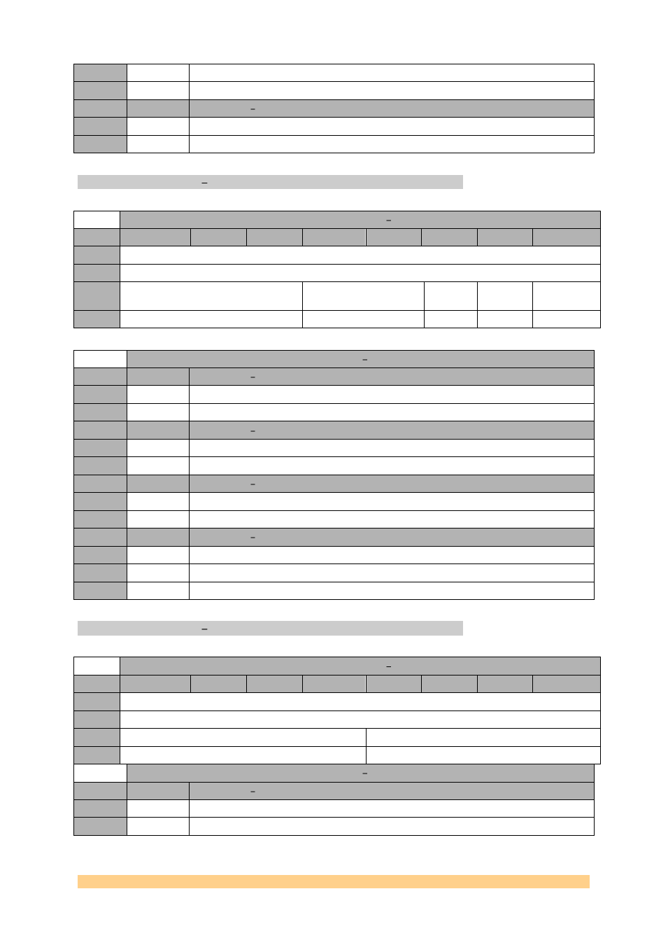
Setting
Bit 15
Description INDET_BP
0
‘0’
Synch logic active when VCXO/AUX clocks are available
1
‘1’
Synch logic is independent from VCXO/AUX
CLOCK Register 13 0x23.
Clock Register 13 0x23
Byte
Bit 7
Bit 6
Bit 5
Bit 4
Bit 3
Bit 2
Bit 1
Bit 0
1
Reserved
Default
‘00000000’
0
Reserved
BIAS_DIV_FB
NPRESET
_MDIV
LOW_FD_
FB_EN
PLL_LOCK_B
P
Default
‘000’
‘00’
‘0’
‘0’
‘0’
Reset Register 13 0x23
Setting
Bit 0
Description PLL_LOCK_BP
0
‘0’
Synch logic waits for the first PLL lock state
1
‘1’
Synch logic independent from first PLL lock state
Setting
Bit 1
Description LOW_FD_FB_EN
0
‘0’
Synch logic is independent from VCXO/DIV_FB frequency
1
‘1’
Synch logic is started for VCXO/DIV_FB > 600khz
Setting
Bit 2
Description NPRESET_MDIV
0
‘0’
M-divider uses nHOLD as NPRESET
1
‘1’
M-divider not preset by nHOLD
Setting
Bit 4:3
Description BIAS_DIV_FB
0
‘00’
No current reduction
1
‘01’
20% current reduction
2
‘10’
30% current reduction
CLOCK Register 14 0x24.
Clock Register 14 0x24
Byte
Bit 7
Bit 6
Bit 5
Bit 4
Bit 3
Bit 2
Bit 1
Bit 0
1
Reference Divider[11:4]
Default
‘00000000’
0
Reference Divider M[3:0]
Reserved
Default
‘0000’
‘1010’
Reset Register 14 0x24
Setting
Bit 11:4
Description Reference Divider M[11:0]
0
1