Register descriptions, 2 control register 0x1 – Sundance SMT943 User Manual
Page 20
User Manual SMT943
Page 20 of 54
Last Edited: 23/08/2011 17:24:00
Register Descriptions
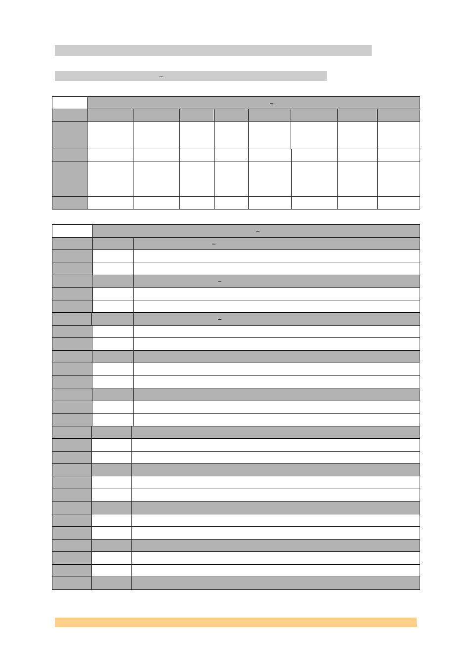
3.3.2 Control Register 0x1.
Control Register 0x01
Byte
Bit 7
Bit 6
Bit 5
Bit 4
Bit 3
Bit 2
Bit 1
Bit 0
1
Sync (chcd)
TxEnable
(chcd)
Trigger
nled
(chcd)
Trigger
nled
(chab)
DCM chcd
reset
DCM chab
reset
Clk_Readb
ack
Default
0
Chcd
trigger
selection
Chdc
internal
trigger
Chab
trigger
selectio
n
Chab
internal
trigger
Chab
Reset
Chcd
update
Chab
update
clk update
Default
‘0’
‘0’
‘0’
‘0’
‘0’
‘0’
‘0’
‘0’
Clock Register 0 0x10
Setting
Bit 0
Description clk update clock chip register update
0
0
No action.
1
1
All clock registers are sent to the clock chip via its serial interface.
Setting
Bit 1
Description chab update channel a and b register update
0
0
No action.
1
1
All registers (chab) are sent to the converter via its serial interface.
Setting
Bit 2
Description chcd update channel c and d register update
0
1
No action.
1
1
All registers (chcd) are sent to the converter via its serial interface.
Setting
Bit 4
Description chab Internal trigger
0
0
No action.
1
1
Starts the data flow (converter chab).
Setting
Bit 5
Description chab trigger selection
0
0
Trigger from control register selected.
1
1
Trigger from external source selected.
Setting
Bit 6
Description chcd Internal trigger
0
0
No action.
1
1
Starts the data flow (converter chcd).
Setting
Bit 7
Description chcd trigger selection
0
0
Trigger from control register selected.
1
1
Trigger from external source selected.
Setting
Bit 8
Description clock readback
0
0
No action.
1
1
Used when read register back from the chip itself.
Setting
Bit 9
Description DCM chab Reset
0
0
No action.
1
1
Resets the DCM used to capture samples from ADC channels.
Setting
Bit 10
Description DCM chcd Reset