Clock register 6 0x16, Clock register 7 0x17 – Sundance SMT943 User Manual
Page 25
User Manual SMT943
Page 25 of 54
Last Edited: 23/08/2011 17:24:00
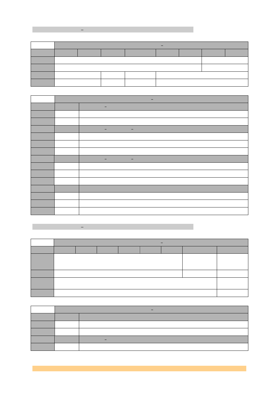
CLOCK Register 6 0x16.
Clock Register 6 0x16
Byte
Bit 7
Bit 6
Bit 5
Bit 4
Bit 3
Bit 2
Bit 1
Bit 0
1
Coarse Phase Adjustment[5:0] (Output DAC cha&b clk2)
BIAS_DIV23
Default
‘000000’
‘00’
0
BIAS_DIV01
Reserved
DIS_FDET_REF
Reserved
Default
‘00’
‘0’
‘0’
‘0011’
Reset Register 6 0x16
Setting
Bit 4
Description DIS_FDET_REF
0
0
Reference Clock detector is ON
1
1
Reference Clock detector is OFF
Setting
Bit 7:6
Description BIAS_DIV01 Current reduction output dividers 0 and 1
0
‘00’
No current output reduction
1
‘01’
20% output current reduction
2
‘10’
30% output current reduction
Setting
Bit 9:8
Description BIAS_DIV23 Current reduction output dividers 2 and 3
0
‘00’
No current output reduction
1
‘01’
20% output current reduction
2
‘10’
30% output current reduction
Setting
Bit 15:10
Description Coarse Phase Adjustment[5:0] DAC cha&b clk1
0
0
1
1
CLOCK Register 7 0x17.
Clock Register 7 0x17
Byte
Bit 7
Bit 6
Bit 5
Bit 4
Bit 3
Bit 2
Bit 1
Bit 0
1
Output0 (DAC cha&b clk2) Mode
PECL3HISWING
Output
Divider
Enable
Default
‘100000’
‘0’
‘0’
0
Output Divider Ratio DAC cha&b clk1 and clk2
Coarse Phase
Adjustment[6]
Default
‘0000000’
‘0’
Reset Register 7 0x17
Setting
Bit 0
Description - Coarse Phase Adjustment[6] DAC cha&b clk2
0
0
1
1
Setting
Bit 7:1
Description Output Divider Ratio DAC cha&b clk2
0
0