Clock register 5 0x15 – Sundance SMT943 User Manual
Page 24
User Manual SMT943
Page 24 of 54
Last Edited: 23/08/2011 17:24:00
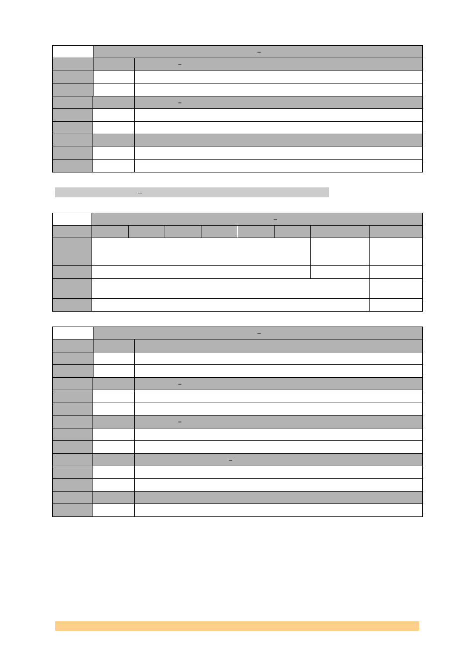
Reset Register 4 0x14
Setting
Bit 6:4
Description Delay M
0
0
1
1
Setting
Bit 9:7
Description Delay N
0
0
1
1
Setting
Bit 15:10
Description Coarse Phase Adjustment[5:0] DAC cha&b clk1
0
0
1
1
CLOCK Register 5 0x15.
Clock Register 5 0x15
Byte
Bit 7
Bit 6
Bit 5
Bit 4
Bit 3
Bit 2
Bit 1
Bit 0
1
Output0 (DAC cha&b clk1) Mode
PECL2HISWING
Output
Divider
Enable
Default
‘100000’
‘0’
‘0’
0
Output Divider Ratio DAC cha&b clk1
Coarse Phase
Adjustment[6]
Default
‘0000000’
‘0’
Reset Register 5 0x15
Setting
Bit 0
Description - Coarse Phase Adjustment[6] DAC cha&b clk1
0
0
1
1
Setting
Bit 7:1
Description Output Divider Ratio DAC cha&b clk1
0
0
1
1
Setting
Bit 8
Description Output Divider Enable DAC cha&b clk1
0
0
Divider disabled.
1
1
Divider enabled.
Setting
Bit 9
Description PECL2HISWING PECL output voltage swing (DAC cha&b clk1)
0
0
Normal Operation.
1
1
High PECL output voltage.
Setting
Bit 15:10
Description Output2 (DAC cha&b clk1) mode
0
0
LVPECL only: ‘100000’.