1 control packet structure, 2 reading and writing registers, 3 fpga design – Sundance SMT943 User Manual
Page 18
User Manual SMT943
Page 18 of 54
Last Edited: 23/08/2011 17:24:00
3.3 FPGA Design
The standard FPGA design implements all the registers described in the followings
parts.
3.3.1 Control Register Settings
The Control Registers control the complete functionality of the SMT943. They are
setup via the Comport3 (standard firmware provided). The settings of the
ADCs/DACs, triggers, clocks and the configuration of the interfaces and the internal
FPGA data path settings can be configured via the Control Registers.
3.3.1.1 Control Packet Structure
The data passed on to the SMT943 over the Comport must conform to a certain
packet structure. Only valid packets will be accepted and only after acceptance of a
packet will the appropriate settings be implemented. Each packet will start with a
command (4 bits – 0x1 for a write operation – 0x2 for a read operation) information,
followed by a register address (12 bits – see table Memory Map), followed by a 16-bit
data. This structure is illustrated in the following figure:
Byte Content
Byte
Bit 7
Bit 6
Bit 5
Bit 4
Bit 3
Bit 2
Bit 1
Bit 0
3
Command
3
Command
2
Command
1
Command
0
Address
11
Address
10
Address 9
Address 8
2
Address 7
Address 6
Address 5
Address 4
Address 3
Address 2
Address 1
Address 0
1
Data 15
Data 14
Data 13
Data 12
Data 11
Data 10
Data 9
Data 8
0
Data 7
Data 6
Data 5
Data 4
Data 3
Data 2
Data 1
Data 0
Figure 15
– Setup Packet Structure.
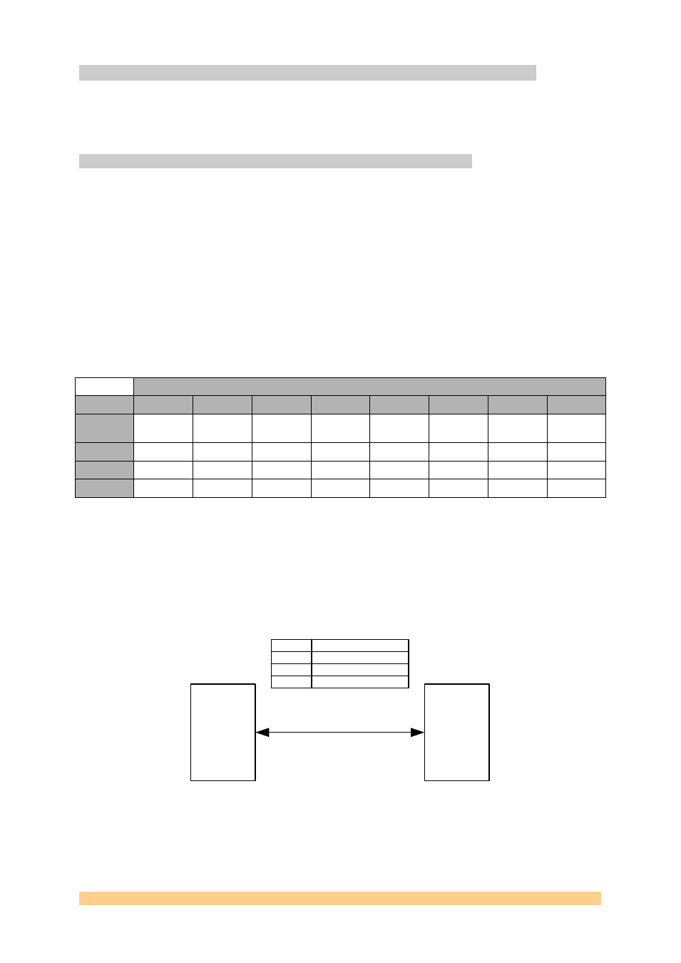
3.3.1.2 Reading and Writing Registers
Control packets are sent to the SMT943 over Comport3. This is a bi-directional
interface. The format of a ‘Read Packet’ is the same as that of a write packet.
Host
Fixed Sequence
SMT942
ComPort 3
Byte 0
Read/Write Address
Byte 1
Read/Write Data
Byte 3
Read/Write Data
Byte 4
1) Write Packet
Figure 16
– Control Register Read Sequence.