Dac chcd phase shift dcm 0x50 – Sundance SMT943 User Manual
Page 50
User Manual SMT943
Page 50 of 54
Last Edited: 23/08/2011 17:24:00
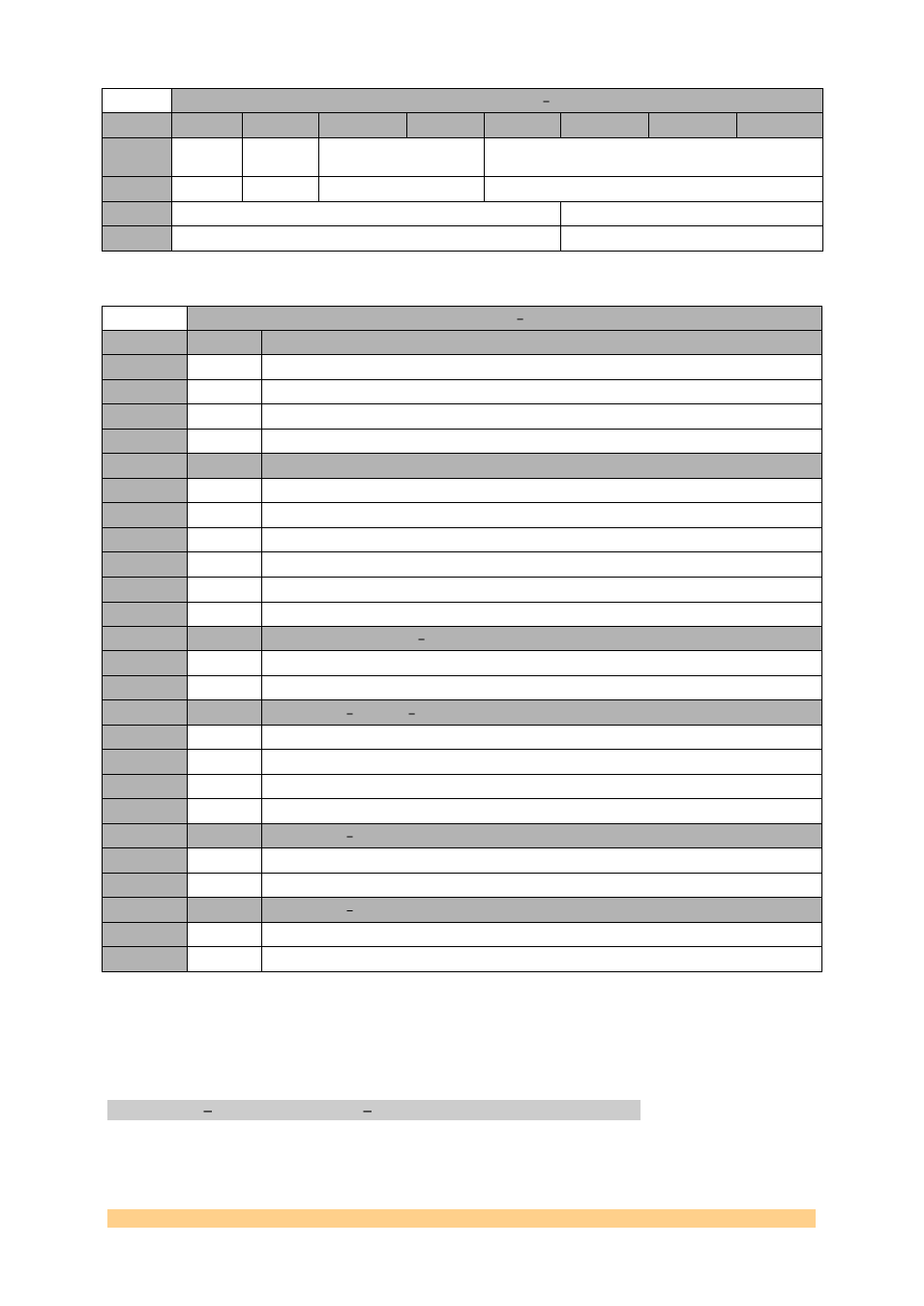
DAC chcd Register E 0x4E
Byte
Bit 7
Bit 6
Bit 5
Bit 4
Bit 3
Bit 2
Bit 1
Bit 0
1
Pll_lpf_r
eset
Vco_div2
Pll_gain
Pll_range
Default
‘0’
‘0’
‘00’
‘0000’
0
Pll_m
Pll_n
Default
‘00000’
‘000’
DAC chcd Register E 0x4E
Setting
Bit 2:0
Description - pll_n
0
‘000’
n value=1.
1
‘001’
n value=2.
2
‘011’
n value=4.
3
‘111’
n value=8.
Setting
Bit 7:3
Description - pll_m
0
‘00000’
m value=1.
1
‘00001’
m value=2.
2
‘00011’
m value=4.
3
‘00111’
m value=8.
4
‘01111’
m value=16.
5
‘11111’
m value=32.
Setting
Bit 11:8
Description - pll_range to adjust the vco current
0
‘0000’
Minimum bias current and lowest VCO frequency range.
1
’1111’
Maximum bias current and highest VCO frequency range.
Setting
Bit 13:12
Description pll_gain to adjust the vco gain (Kvco)
0
‘00’
1
‘01’
2
‘10’
3
‘11’
Setting
Bit 14
Description vco_div2
0
‘0’
PLL clock output is not divided.
1
’1’
PLL clock output is divided by 2.
Setting
Bit 15
Description pll_lpf_reset
0
‘0’
1
’1’
Holds the pll loop filter at 0 volts
DAC Chcd Phase shift DCM 0x50.