4 insert data output (j4), 5 drop data input (j5), 6 drop data output (j6) – Comtech EF Data SDM-309B User Manual
Page 114: 7 insert data input (j7), 8 insert data output (j8), 9 external reference clock (j9)

SDM-309B Satellite Modem
M&C and Interfaces
MN/U-SDM309B Rev. #
4-4–37
Note: The balanced insert data input signals on J3 are selected by SW2. Refer to Section
4.2.2.11.3 for further balanced insert data signal selection information.
4.2.2.10.4 Insert Data Output (J4)
The balanced Insert Data Output is provided on a 15 pin female "D" connector and is
located on the front of the break-out panel. Screw locks are provided for mechanical
security of the mating connector.
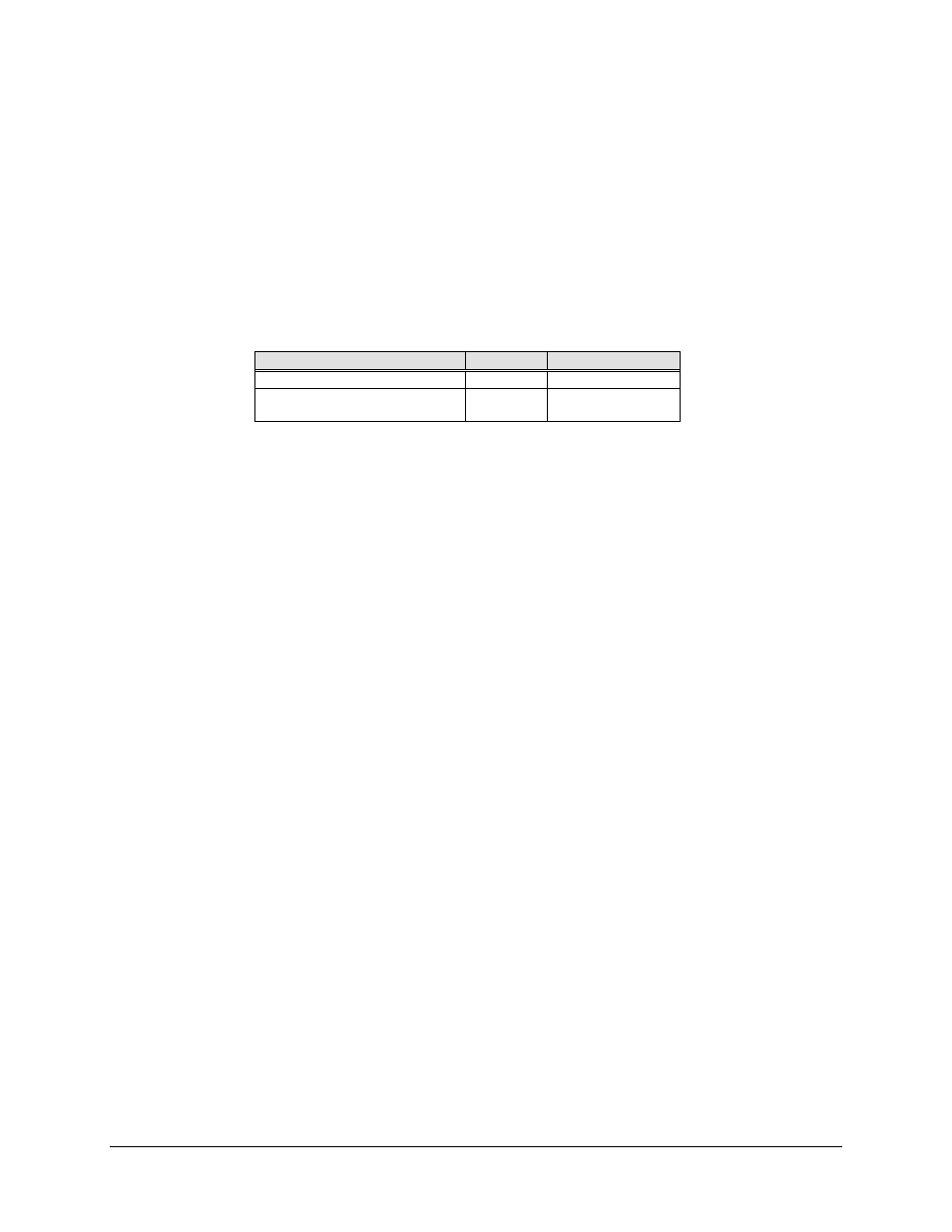
Signal Function
Name
Pin Number
GROUND
GND
2, 4
INSERT DATA OUTPUT
IDO-A
IDO-B
3
11
Note: The balanced insert data output signals on J4 are selected by SW2. Refer to
Section 4.2.2.11.4 for further balanced insert data output signal selection information.
4.2.2.10.5 Drop Data Input (J5)
This connector is the interface for the unbalanced drop data input. The unbalanced drop
data input signal on J5 is selected by SW1. Refer to Section 4.2.2.11.1 for further
information on selecting the balanced or unbalanced drop data input signal.
4.2.2.10.6 Drop Data Output (J6)
This connector is the interface for the unbalanced drop data output. The unbalanced drop
data output signal on J6 is selected by SW1. Refer to Section 4.2.2.11.2 for further
information on selection of the balanced or unbalanced drop data output signal.
4.2.2.10.7 Insert Data Input (J7)
This connector is the interface for the unbalanced insert data input. The unbalanced
insert data input signal on J7 is selected by SW2. Refer to Section 4.2.2.11.3 for further
information on selection of the balanced or unbalanced insert data input signal.
4.2.2.10.8 Insert Data Output (J8)
This connector is the interface for the unbalanced insert data output. The unbalanced
insert data output signal on J8 is selected by SW2. Refer to Section 4.2.2.11.4 for further
information on selection of the balanced or unbalanced insert data output signal.
4.2.2.10.9 External Reference Clock (J9)
