Development board block diagram, Handling the board – Altera Cyclone V E FPGA Development Board User Manual
Page 8
1–4
Chapter 1: Overview
Development Board Block Diagram
Cyclone V E FPGA Development Board
March 2013
Altera Corporation
Reference Manual
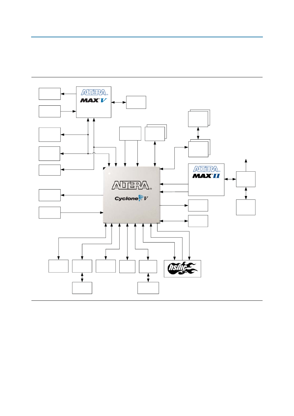
Development Board Block Diagram
shows a block diagram of the Cyclone V E FPGA development board.
Handling the Board
When handling the board, it is important to observe the following static discharge
precaution:
c
Without proper anti-static handling, the board can be damaged. Therefore, use
anti-static handling precautions when touching the board.
Figure 1–1. Cyclone V E FPGA Development Board Block Diagram
5CEFA7F31I7N
N
Data x 16
Addr x 25
Control x 23
2.5V
JTAG Chain
LEDs
Clock In
125 M, 50 M
Clock In
100 M, 50 M
Debug
Header
DSUB 9-pin
Connector
x5
x1
x2
EPCQ
5M2210ZF256I5N
CLKIN x3
CLKOUT x3
LVDS/Single-Ended
Type-A USB
Connector
x80
2.5 V
x31
2.5 V
x6
2.5 V
x4
2.5 V
x4
2.5 V
x16 2.5 V
x16 1.5 V
x16 HSUL 1.2
x22
RGMII
2.5 V
x19 USB
Interface 2.5 V
x32
SSTL - 15
x11
2.5 V
x4
3.3 V
x2
3.3 V
USB-to-
UART
LCD
Character
32 Kb
UART
32 Kb
EEPROM
SMA
Clock Out
18 Mb
SSRAM
512 Mb
Flash
Clock Enable
Fan
Connector
AS x1,x4
FPP x16
Configuration
Buttons &
Switches
2 x 256 MB
DDR3
EPM570GM100I5N
Embedded
USB-Blaster II
2 x RJ-45
LAN
Connector
USB CLK to
Cyclone V
and MAX V
Cypress
USB 2.0
Controller
Type-B
USB
Connector
512 MB
LPDDR2
2x Gigabit
Ethernet PHY